Light emitting diode and manufacturing method thereof

a technology of light-emitting diodes and manufacturing methods, which is applied in the direction of semiconductor/solid-state device manufacturing, electrical equipment, semiconductors, etc., can solve the problems of low efficiency, complicated fabrication process of ts algainp led, and disadvantages of conventional technologies, so as to increase light extraction efficiency and light-emitting efficiency

Inactive Publication Date: 2009-02-05
CHI MEI LIGHTING TECH
View PDF12 Cites 38 Cited by
  • Summary
  • Abstract
  • Description
  • Claims
  • Application Information

AI Technical Summary

Benefits of technology

[0013]Therefore, with the application of the light emitting diode disclosed in the embodiments of the present invention, the light emitting diode of the present invention can use the refraction dielectric layer to refract the inner light thereof, thereby increasing the light extraction efficiency and the light emitting efficiency.

Problems solved by technology

However, these conventional technologies still have some disadvantages and limitations.
However, because the DBR layer only reflects light that is of near normal incidence to the GaAs substrate, the efficiency is not very great.
However, the fabrication process of TS AlGaInP LED is too complicated.
Therefore, it is difficult to manufacture these TS AlGaInP LEDs in high yield and low cost.

Method used


Image

  • Light emitting diode and manufacturing method thereof
  • Light emitting diode and manufacturing method thereof
  • Light emitting diode and manufacturing method thereof

Examples


Embodiment Construction

[0020]In order to make the illustration of the present invention more explicit and complete, the following description is stated with reference to FIG. 1A through FIG. 5B.

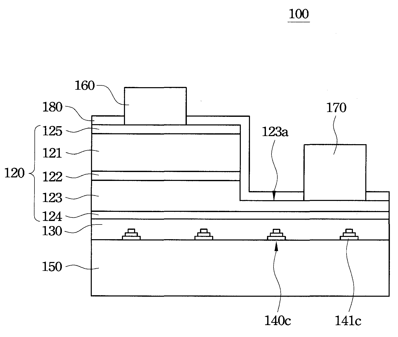
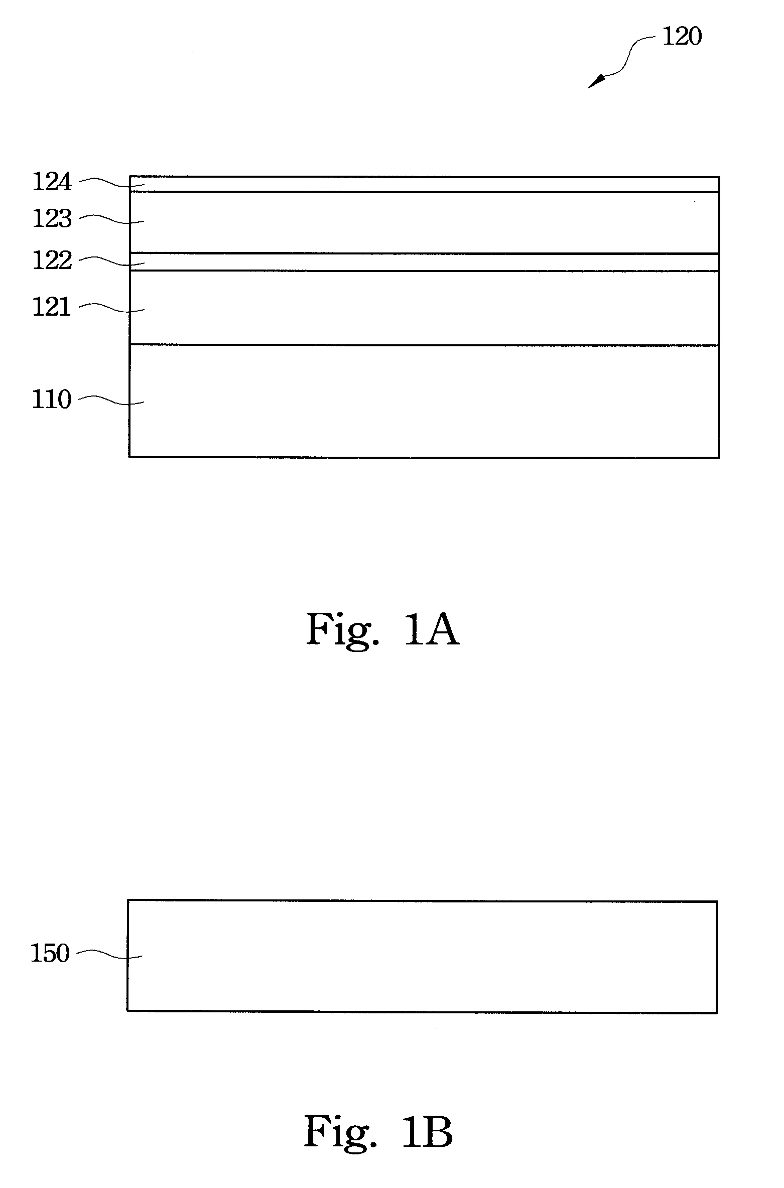
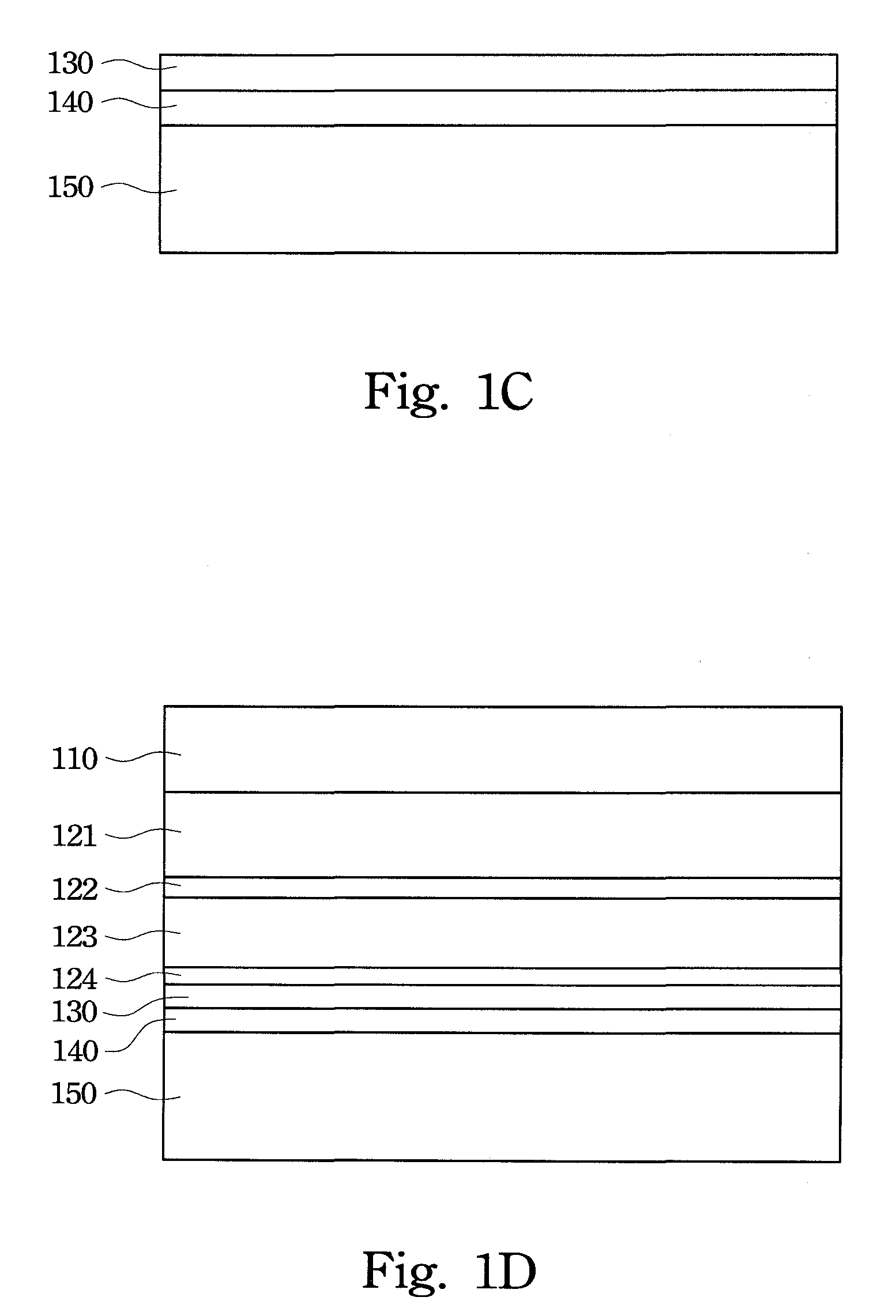
[0021]Refer to FIG. 1A through FIG. 1F. FIG. 1A through FIG. 1F are schematic flow diagrams showing the process for manufacturing a light emitting diode according to a first embodiment of the present invention. The light emitting diode 100 of the first embodiment comprises an epitaxy structure 120, a bonding layer 130, a refraction dielectric layer 140, a transparent substrate 150, a first electrode 160, a second electrode 170, and an insulating protecting layer 180. The refraction dielectric layer 140, bonding layer 130 and epitaxy structure 120 are stacked on the transparent substrate 150 in sequence, wherein the epitaxy structure 120 has a first conductivity type semiconductor layer 121, an active layer 122, a second conductivity type semiconductor layer 123, a second conductivity type contact layer 124 and a fi...


PUM

PropertyMeasurementUnit
refractive indexaaaaaaaaaa
luminous intensityaaaaaaaaaa

Abstract

A light-emitting diode and the manufacturing method thereof are disclosed. The manufacturing method comprises the steps of: sequentially forming a refraction dielectric layer, a bonding layer, an epitaxy structure and a first electrode on a permanent substrate, wherein the epitaxy structure comprises a first conductivity type semiconductor layer, an active layer and a second conductivity type semiconductor layer stacked in sequence; and forming a second electrode on the portion surface of the second conductivity type semiconductor layer. Therefore the light-emitting diode is achieved.

Description

RELATED APPLICATIONS[0001]The present application is based on, and claims priority from, Taiwan Application Serial Number 96128760, filed Aug. 3, 2007, the disclosure of which is hereby incorporated by reference herein in its entirety.FIELD OF THE INVENTION[0002]This invention relates to a lead frame structure of a light emitting diode and a manufacturing method thereof, and more particularly, to a light emitting diode with high light extraction efficiency and a manufacturing method thereof.BACKGROUND OF THE INVENTION[0003]A light emitting diode (LED) is composed of an epitaxial structure such as a homo-structure, a single hetero-structure, a double hetero-structure or a multiple quantum well. The LED with a p-n junction interface that can emit light with various wavelengths has several beneficial characteristics, including low electrical power consumption, low heat generation, long operational life, small volume, good impact resistance, fast response and excellent stability. These ...

Claims


Application Information

Patent Timeline
Patent Type & Authority Applications(United States)
IPC IPC(8): H01L33/00H01L21/311H01L33/22H01L33/44
CPCH01L33/0079H01L33/44H01L33/22H01L33/0093
Inventor LI, KUO-YUIN
Owner CHI MEI LIGHTING TECH
Why Eureka
Try Eureka