Magnetic field detecting apparatus

a magnetic field and detecting device technology, applied in the direction of magnetic measurement, instruments, measurement devices, etc., can solve the problems of very hardly adding and setting test modes, and achieve the effect of performing an investigation within a short time without increasing the chip size and low power consumption of the magnetic field detecting apparatus

Inactive Publication Date: 2009-02-05
COLLABO INNOVATIONS INC
View PDF0 Cites 16 Cited by
  • Summary
  • Abstract
  • Description
  • Claims
  • Application Information

AI Technical Summary

Benefits of technology

[0015]An object of the present invention is to provide a magnetic field detecting apparatus capable of performing an investigation within a short time without increasing a chip size and a total quantity of terminals, while power consumption of the magnetic field detecting apparatus is low.
[0031]In accordance with the present invention, it is possible to provide the magnetic field detecting apparatus capable of performing an investigation within a short time without increasing a chip size and a total quantity of terminals, while power consumption of the magnetic field detecting apparatus is low.

Problems solved by technology

However, due to such a reason that the above-described Hall IC is a miniature chip and the miniature Hall IC has no input pin for a mode selection purpose, the test mode can be very hardly added and set.

Method used


Image

  • Magnetic field detecting apparatus
  • Magnetic field detecting apparatus
  • Magnetic field detecting apparatus

Examples


first embodiment

Mode

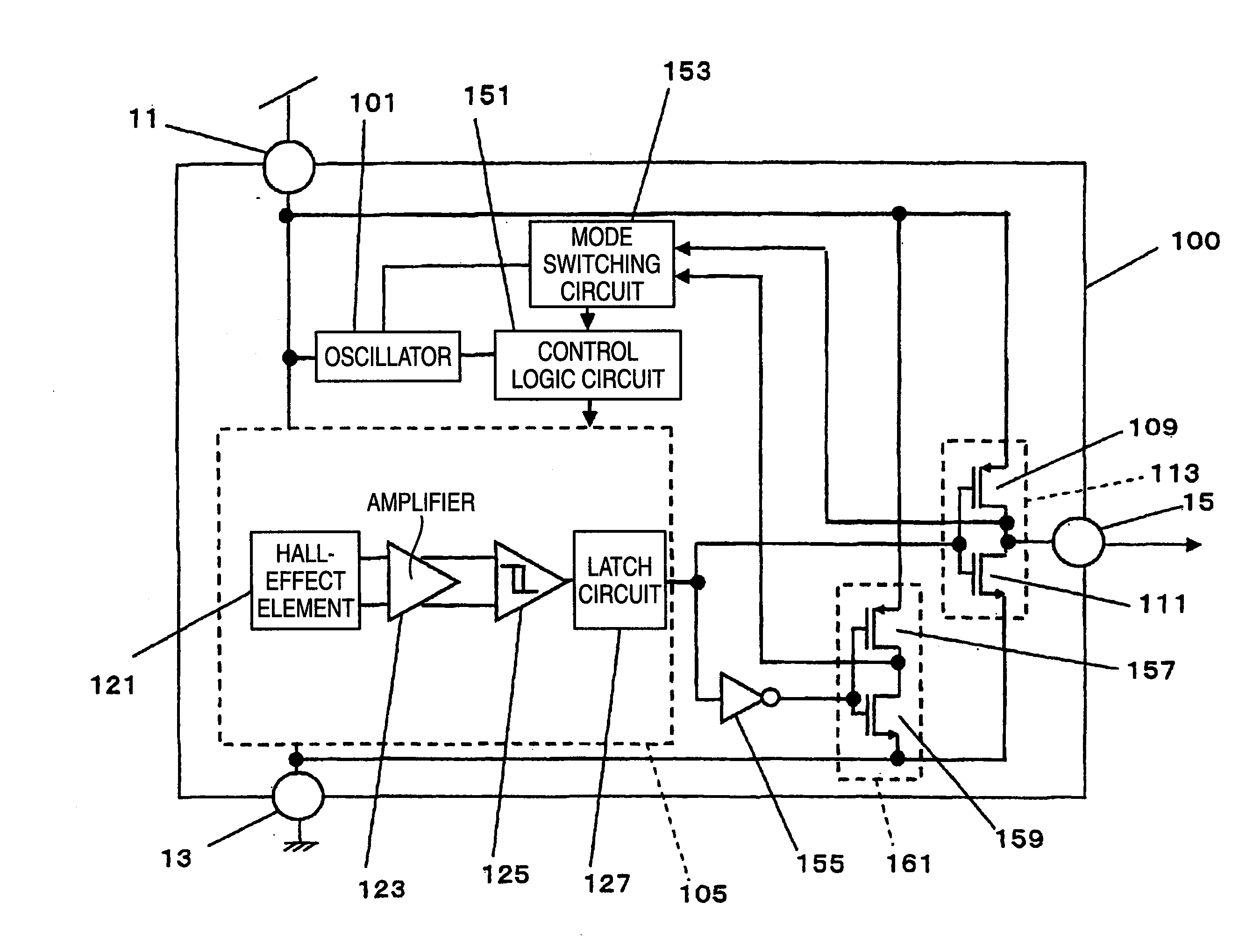
[0050]FIG. 1 is a block diagram for showing a Hall IC 100 according to a first embodiment mode of the present invention. It should also be noted that in FIG. 1, the same reference numerals shown in FIG. 1 have been applied to structural elements similar to those provided in the Hall IC 10 of FIG. 16, which have been described in the Background Art. As indicated in FIG. 1, the Hall IC 100 of the first embodiment mode is equipped with a power supply terminal 11, a GND terminal 13, an output terminal 15, an oscillator 101, a control logic circuit 151, a magnetic field detecting circuit 105, a mode switching circuit 153, an output inverter circuit 113, an inverter 155, and another output inverter unit 161. In the output inverter circuit 113, an NMOS 109 and a PMOS 111 have been series-connected to each other. In the output inverter circuit 161, an NMOS 157 and a PMOS 159 have been series-connected to each other.

[0051]A gate of the NMOS 109 and a gate of the PMOS 111 have been common...

second embodiment

Mode

[0080]FIG. 11 is a block diagram for showing a Hall IC 200 according to a second embodiment mode of the present invention. The Hall IC 200 of the second embodiment mode has the below-mentioned different points, as compared with those of the Hall IC 100 of the first embodiment mode: That is, the Hall IC 200 is equipped with an output terminal connected to the common drain of the output inverter circuit 161; the Hall IC 200 is not provided with the above-described inverter 155; and a magnetic field detecting circuit 205 separately outputs a Hall voltage (will be referred to as “S-pole Hall voltage” hereinafter) in response to magnetic flux density (otherwise magnetic field) of an S pole, and another Hall voltage (will be referred to as “N-pole Hall voltage” hereinafter) in response to magnetic flux density (otherwise magnetic field) of an N pole, the S-pole Hall voltage is applied to the common gate of the output inverter circuit 113, and also, the N-pole Hall voltage is applied t...

third embodiment

Mode

[0086]FIG. 14 is a block diagram for showing a Hall IC 300 according to a third embodiment mode of the present invention. As indicated in FIG. 14, similar to the first embodiment mode, the Hall IC 300 of the third embodiment mode is equipped with a power supply terminal 11, a GND terminal 13, an output terminal 15, an oscillator 101, a control logic circuit 151, a magnetic field detecting circuit 105, an output inverter circuit 113, a mode switching circuit 353, and a reference voltage generating unit 301. The Hall IC 300 of the third embodiment mode is not equipped with the above-described inverter 155, but also, the mode switching circuit 353 has not been connected to the common drain of the output inverter circuit 113.

[0087]FIG. 15 is a circuit diagram for showing the mode switching circuit 353 provided in the Hall IC 300 of the third embodiment mode. As indicated in FIG. 15, the mode switching circuit 353 of this third embodiment mode contains resistors 401 and 402, and a co...


PUM


Abstract

The magnetic field detecting apparatus is provided with: a magnetic field detecting unit for outputting one of two signals having different potential levels from each other in response to a perpheral magnetic field; an energizing control unit for producing a periodic energizing control signal indicative of timing at which the magnetic field detecting unit is energized by employing a clock signal and another signal obtained by frequency-dividing, or frequency-multiplying the clock signal, and for supplying the produced energizing control signal to the magnetic field detecting unit; a first inverting unit for inverting the potential level of the output signal of the magnetic field detecting unit; and an energizing time period control unit for supplying a time period control signal to the energizing control unit, the time period control signal controlling the time period of the energizing control signal in response to the potential level of the output signal of the magnetic field detecting unit, and the potential level of the signal obtained by inverting the potential level of the output signal by the first inverting unit. The energizing time period control unit supplies any one of two pieces of the energizing control signals whose durations and time periods are different from each other, during which the magnetic field detecting unit is not energized, in response to the potential level of the time period control signal supplied from the energizing time period control unit.

Description

BACKGROUND OF THE INVENTION[0001]1. Field of the Invention[0002]The present invention is related to a magnetic field detecting apparatus for intermittently detecting a magnetic field, and also, related to an electronic appliance containing the above-described magnetic field detecting apparatus.[0003]2. Description of the Related Art[0004]As one of magnetic field detecting apparatuses, Hall ICs utilizing Hall-effect elements have been proposed. Also, among these Hall ICs, there are some Hall ICs equipped with intermittent driving functions in order to achieve low power consumption (refer to non-patent publication 1).[0005]FIG. 16 is a block diagram for showing a Hall IC 10 equipped with an intermittent driving function. As shown in FIG. 16, the Hall IC 10 is provided with a power supply terminal 11, a GND terminal 13, an output terminal 15, an oscillator 101, a control logic circuit 103, a magnetic field detecting circuit 105, and an output inverter circuit 113. In the output inverte...

Claims


Application Information

Patent Timeline
Patent Type & Authority Applications(United States)
IPC IPC(8): G01R33/00
CPCG01R33/07
Inventor TOMIDA, TAKUYAHATANAKA, TADATAMASAI, SHIGEO
Owner COLLABO INNOVATIONS INC
Why Eureka
Try Eureka