Comparator with low supplies current spike and input offset cancellation
a technology of low supply current and comparator, applied in the direction of electrical equipment, amplifiers, pulse manipulation, etc., can solve the problems of large current spikes of comparator on one or both voltage supplies, significant noise, and interference with chip operation
- Summary
- Abstract
- Description
- Claims
- Application Information
AI Technical Summary
Benefits of technology
Problems solved by technology
Method used
Image
Examples
Embodiment Construction
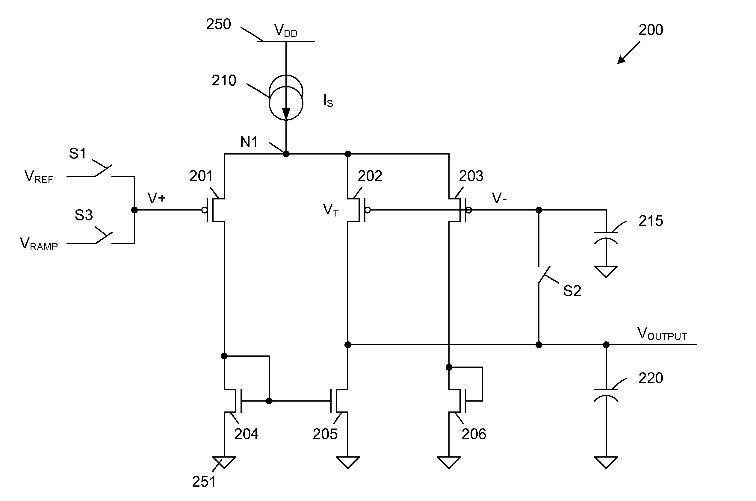
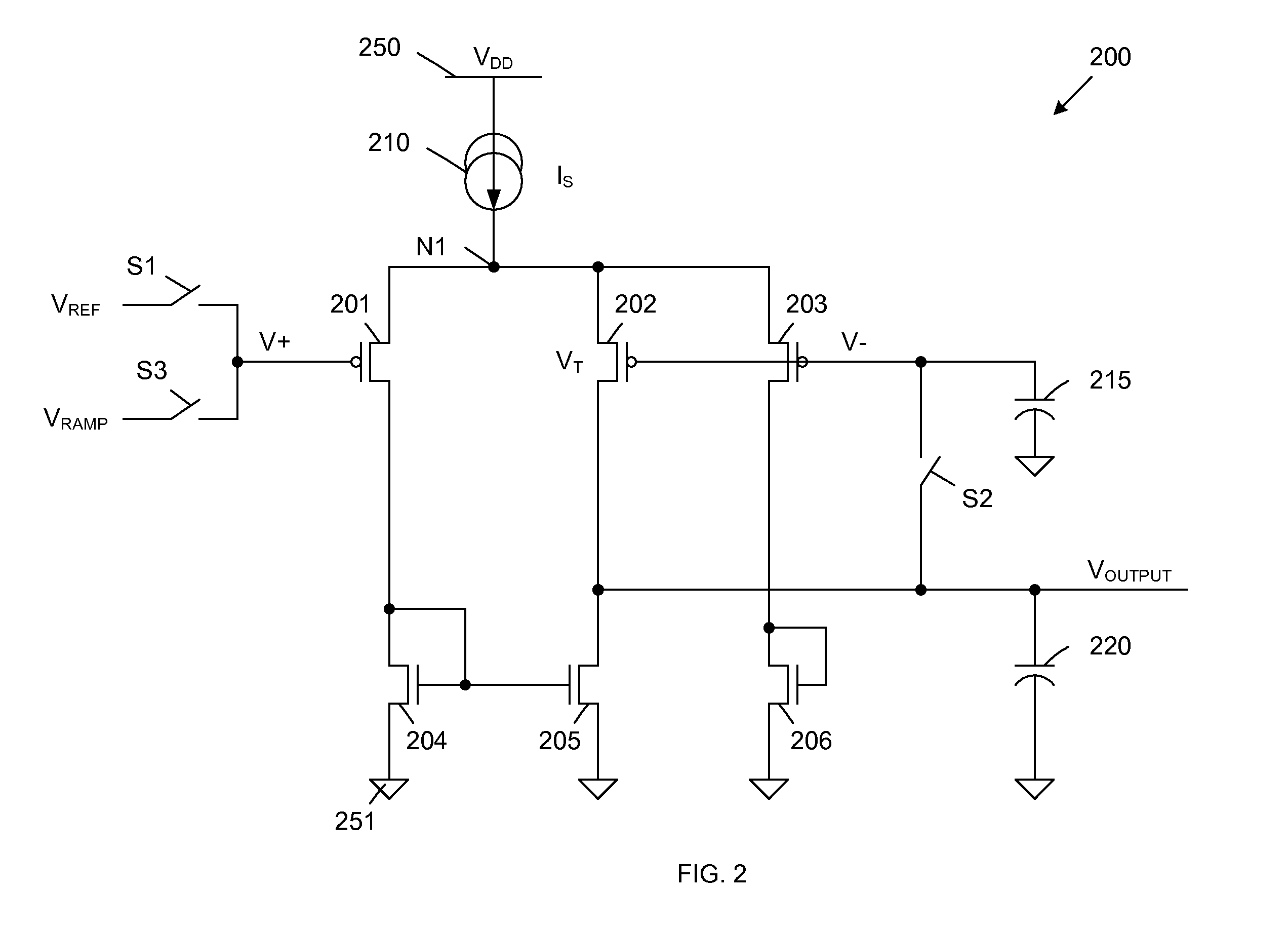
[0014]FIG. 2 is a circuit diagram of a comparator 200 in accordance with one embodiment of the present invention. Comparator 200 includes PMOS transistors 201-203, NMOS transistors 204-206, current source 210, sample capacitor 215, output capacitor 220 and switches S1-S3. Comparator 200 is supplied by a VDD voltage supply 250 and a ground voltage supply 251. These voltage supplies 250-251 effectively form a current source 210, which provides a source current (IS) to node N1.
[0015]As described in more detail below, PMOS transistors 201-202 and NMOS transistors 204-205 form a differential comparator circuit, which provides an output voltage (VOUTPUT) in response to the voltages (V+, V−) applied to the gates of PMOS transistors 201 and 202. PMOS transistor 203 and NMOS transistor 206 form a current control circuit, which is coupled in parallel with the current paths of the differential comparator circuit, and ensures that a substantially constant current is drawn from current source 21...
PUM
 Abstract
Description
Claims
Application Information


