Flip chip type light-emitting element

a chip and light-emitting element technology, applied in the direction of basic electric elements, electrical equipment, semiconductor devices, etc., can solve the problems of light transmission electrodes deteriorating the light transmission electrod

Active Publication Date: 2009-02-12
TOYODA GOSEI CO LTD
View PDF14 Cites 39 Cited by
  • Summary
  • Abstract
  • Description
  • Claims
  • Application Information

AI Technical Summary

Benefits of technology

[0012]Thus, it is an object of the present invention to realize a flip chip type light-emitting element in which the deterioration of a light transmission electrode is suppressed.

Problems solved by technology

However, in the flip chip type light-emitting element having a light transmission electrode on the surface of a p layer and a plurality of pad electrodes provided on the light transmission electrode, a problem arises that since the areas of the pad electrodes are small, an electric current is concentrated on the contact parts of the pad electrodes and the light transmission electrode to deteriorate the light transmission electrode.

Method used


Image

  • Flip chip type light-emitting element
  • Flip chip type light-emitting element
  • Flip chip type light-emitting element

Examples


first embodiment

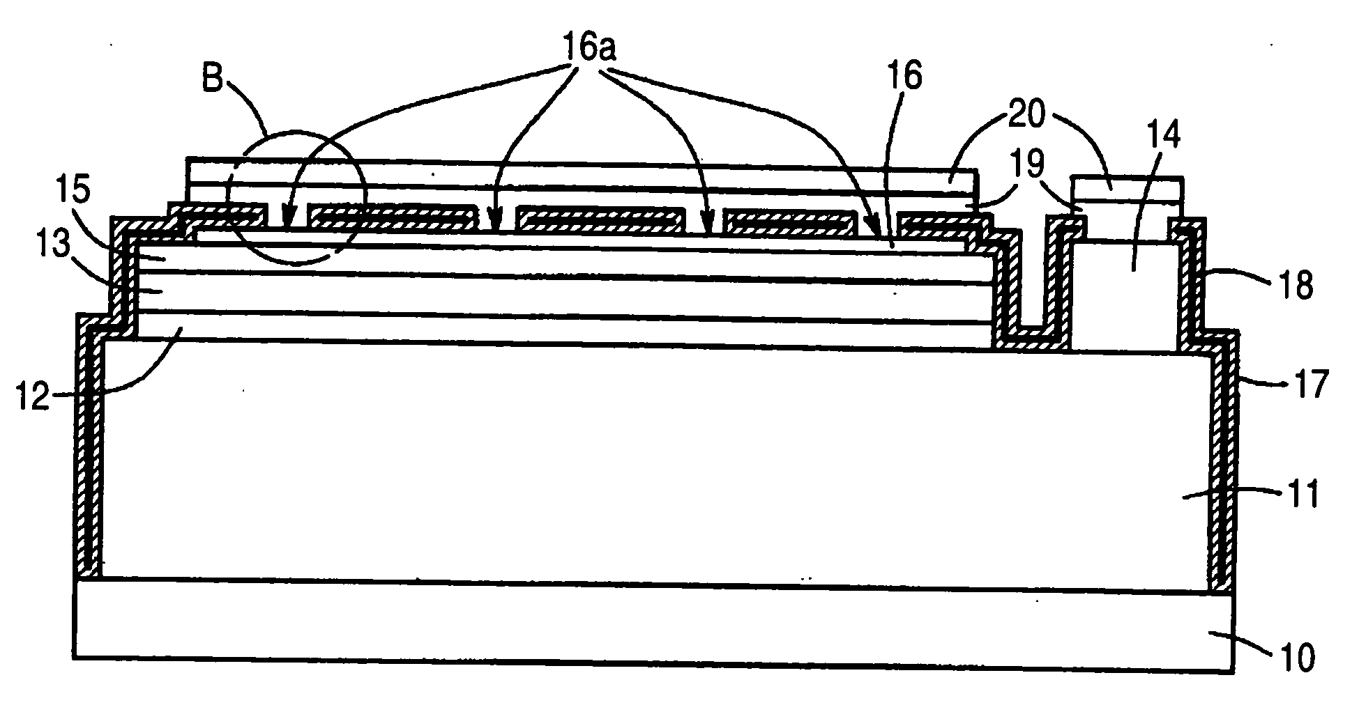
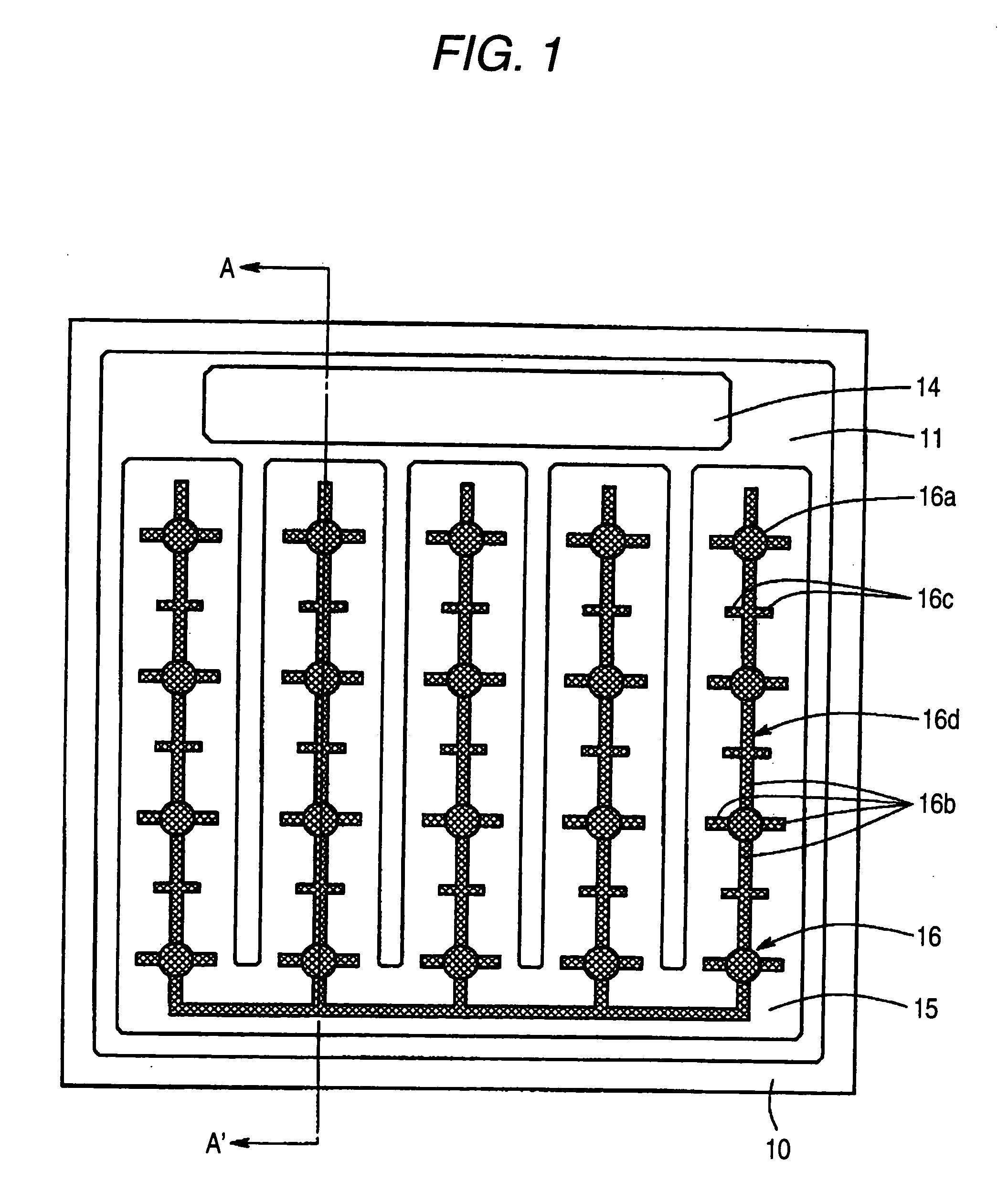
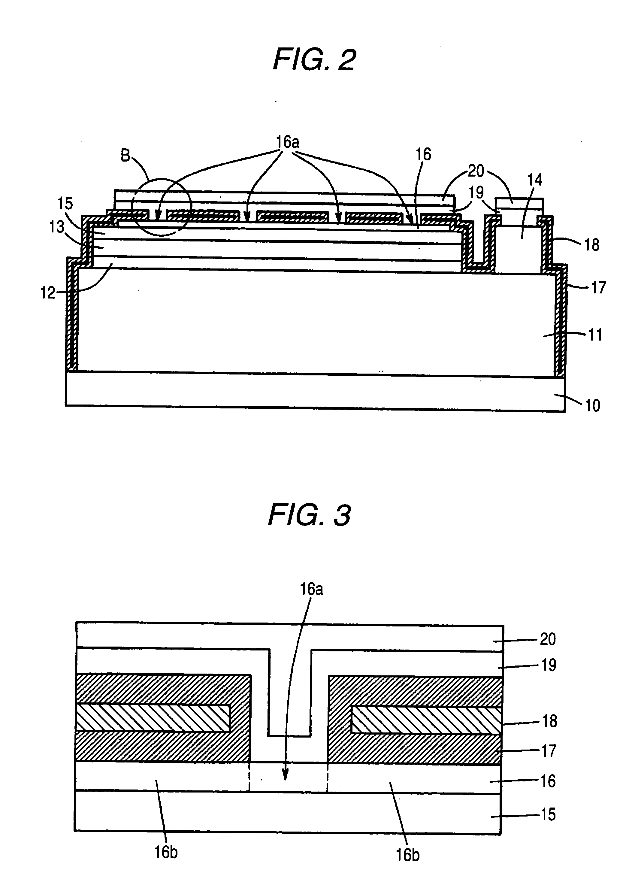
[0035]FIG. 1 is a plan view showing the structure of a flip chip type light-emitting element of a first embodiment. FIG. 2 is a sectional view taken along a line A-A′ in FIG. 2. FIG. 3 is an enlarged view of a part B in FIG. 2.

[0036]The flip chip type light-emitting element mainly includes a III-group nitride semiconductor layer (an n layer 11, an active layer 12, a p layer 13) formed on a sapphire substrate 10 through a buffer layer (not shown in the drawing) and an electrode (an n type contact electrode 14, a light transmission electrode 15, a pad electrode 16) connected thereto.

[0037]The III-group nitride semiconductor layer has a structure that the n layer 11, the active layer 12 and the p layer 13 are laminated in order. The n layer has a structure that the n type contact layer composed of GaN doped with Si to a high concentration and an n clad layer composed of GaN are laminated in order. The p layer 13 has a structure that a p clad layer composed of AlGaN doped with Mg and a ...


PUM


Abstract

In a flip chip type light-emitting element of the present invention, an n type contact electrode 14 is formed on an n layer 11 exposed in a comb-tooth shape, a light transmission electrode 15 made of an ITO is formed over the entire surface of an upper surface of a p layer 13 and twenty pad electrodes 16 are formed at prescribed intervals on the light transmission electrode 15. The plane form of the pad electrode 16 has four branches 16b protruding in the form of a cross from a circular central part 16a and the adjacent pad electrodes 16 connected to each other by the branches 16b.

Description

BACKGROUND OF THE INVENTION[0001]1. Field of the Invention[0002]The present invention relates to a flip chip type light-emitting element formed with a III-group nitride semiconductor, and more particularly to a flip chip type light-emitting element having a feature in the form of an electrode.[0003]2. Description of the Related Art[0004]In recent years, various techniques are made use of to suppress unevenness in light transmission by uniformly supplying an electric current to a light-emitting layer in the flip chip type light-emitting element formed with the III-group nitride semiconductor.[0005]For instance, as a technique for improving the diffusion characteristics of a current to a light-emitting layer, a technique that an n layer is exposed in a comb-tooth shape and an n type contact electrode is provided in the exposed part is disclosed in Patent Documents 1 and 2. Further, Patent Documents 2 and 3 disclose a technique that a light transmission electrode is provided on the ent...

Claims


Application Information

Patent Timeline
Patent Type & Authority Applications(United States)
IPC IPC(8): H01L33/00H01L33/06H01L33/10H01L33/22H01L33/32H01L33/38H01L33/42H01L33/62
CPCH01L33/387H01L33/46H01L33/44
Inventor YAHATA, KOSUKENAKAJO, NAOKI
Owner TOYODA GOSEI CO LTD
Why Eureka
Try Eureka