Thin film transistor, pixel structure and liquid crystal display panel

a technology of thin film transistors and liquid crystal display panels, applied in semiconductor devices, instruments, electrical devices, etc., can solve the problems of inability difficult to reduce the thickness and often occur misalignment in the process of assembling the two substrates, so as to reduce the manufacturing cost of the liquid crystal display panel

Active Publication Date: 2009-02-12
AU OPTRONICS CORP
View PDF16 Cites 39 Cited by
  • Summary
  • Abstract
  • Description
  • Claims
  • Application Information

AI Technical Summary

Benefits of technology

[0008]The present invention is directed to a thin film transistor, wherein a light shows a specific color after passing through the insulating film layers of the thin fil...

Problems solved by technology

However, fabricating the color filter array and the pixel array in different processes complicates the manufacturing process of the liquid display panel.
Besides, it is impossible to reduce the thickness of the liquid crystal display panel because manufactur...

Method used


Image

  • Thin film transistor, pixel structure and liquid crystal display panel
  • Thin film transistor, pixel structure and liquid crystal display panel
  • Thin film transistor, pixel structure and liquid crystal display panel

Examples


Embodiment Construction

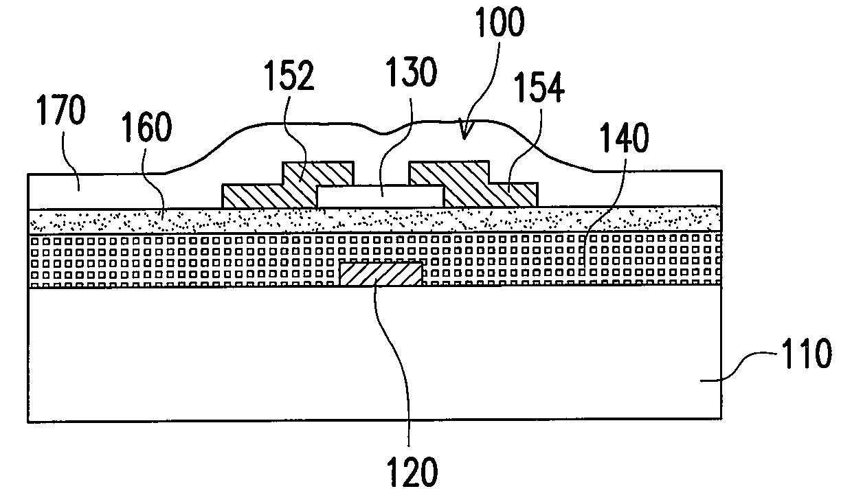
[0053]In a conventional thin film transistor, an insulating layer or multiple insulating layers must be disposed for electrically insulating a gate from a source, a drain and a channel layer. Due to the fact that a variety of insulating materials can have a color-changing effect or a light-filtering effect, the present invention is directed to fabricating the insulating film layer of a thin film transistor and a pixel structure by using such insulating materials. Therefore, the light can show a specific color after passing through the thin film transistor, the pixel structure and related devices of the present invention.

[0054]FIG. 1 illustrates a thin film transistor according to an embodiment of the present invention. Referring to FIG. 1, a thin film transistor 100 is disposed on a substrate 110. The thin film transistor 100 includes a gate 120, a semi-conductive layer 130, a gate insulator 140, a source 152 and a drain 154. The gate insulator 140 disposed between the gate 120 and ...


PUM


Abstract

A thin film transistor disposed on a substrate is provided. The thin film transistor includes a gate, a semi-conductive layer, a gate insulator, a source and a drain. The gate insulator is located between the gate and the semi-conductive layer. A light shows a specific color after passing through the gate insulator. The source and the drain are disposed on the semi-conductive layer. A pixel structure and a liquid crystal display panel having the pixel structure are also provided. The liquid crystal display panel can display colorful images without disposing a color filter array additionally so that the manufacturing process of the liquid crystal panel is simple and the manufacturing cost of the liquid crystal panel is low.

Description

CROSS-REFERENCE TO RELATED APPLICATION[0001]This application claims the priority benefit of Taiwan application serial no. 96129596, filed on Aug. 10, 2007. All disclosure of the Taiwan application is incorporated herein by reference.BACKGROUND OF THE INVENTION[0002]1. Field of the Invention[0003]The present invention relates to a thin film transistor, a pixel structure and a liquid crystal display panel using the thin film transistor and the pixel structure. In particular, the present invention relates to a thin film transistor and a pixel structure having a color-changing effect or a light-filtering effect, and a liquid crystal display panel using the thin film transistor and the pixel structure.[0004]2. Description of Related Art[0005]In recent years, with great advance in the fabricating technique of electrical-optical and semiconductor devices, flat panel displays (FPDs) have been developed rapidly. Due to the advantages of a liquid crystal display, for example, a low operation ...

Claims


Application Information

Patent Timeline
IPC IPC(8): H01L31/02
CPCG02F1/133345G02F1/133514G02F2001/136222G02F1/133617G02F2202/046G02F2202/36G02F1/1368G02F1/136222
Inventor CHUANG, CHIAO-SHUNCHEN, FANG-CHUNGSHIEH, HAN-PING DAVID
Owner AU OPTRONICS CORP
Why Eureka
Try Eureka