
Flat- panel display device and electronic apparatus

a technology of electronic equipment and display devices, which is applied in the direction of instruments, computing, electric digital data processing, etc., can solve the problems of increasing the thickness of the device itself, increasing the cost, and reducing the display quality, so as to improve the s/n ratio of the position detection signal, and reduce the cost of the signal processing circuit.

Active Publication Date: 2009-02-12
NEC LCD TECH CORP
View PDF6 Cites 49 Cited by
  • Summary
  • Abstract
  • Description
  • Claims
  • Application Information

AI Technical Summary

Benefits of technology

[0025]It is a first object of the present invention to provide a combination touch sensor / flat-panel display device that is light in weight, small in size, suited to a reduction in thickness and free of any decline in display characteristics.
[0026]It is a second object of the present invention to provide this flat-panel display device at low cost.
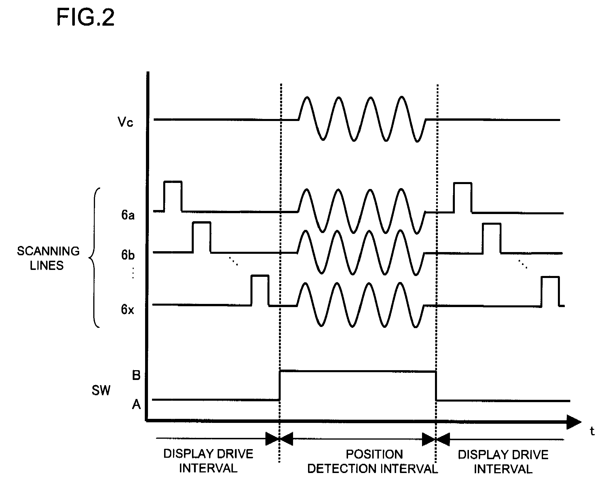
[0033]In accordance with the present invention, at least one wire or electrode disposed from the exterior to the interior of the display area from among wires or electrodes for applying electrical signals to a display element is placed at a high impedance in an interval over which the current detecting circuit detects current. As a result, the S / N ratio of a position detection signal is greatly improved. Further, the cost of the signal processing circuit can be reduced owing to this great improvement in the S / N ratio of the position detection signal. Further, switching elements on the display device substrate are held in the off state so that there is no decline in display characteristics.
[0034]Further, in accordance with the present invention, the impedance surface performs the role of a transparent conductive film in a surface-capacitive touch sensor. This means that the display device need not be provided separately with a surface-capacitive touch sensor, the thickness of the device can be reduced and resources can be conserved.

Problems solved by technology

With such an arrangement, however, the fact that the touch sensor exists on the display surface results in certain problems, namely an increase in the thickness of the device itself, a rise in cost and a decline in display quality.
As a result, it is maintained that the problems of an increase in the thickness of the device itself, a rise in cost and a decline in display quality are solved.
According to the inventor's analyses, the display devices disclosed in Patent Documents 3 and 4 involve several problems.
A first problem is that the signal quantity relating to the position pointed at or concerning whether a pointing operation has been performed is small.
Since the human body does not have a well-defined ground, it is difficult to determine the capacitance (impedance) of a finger by computation and experimentation, therefore, is important.
A second problem is that a signal that is not related to a position pointed at or not related to whether a pointing operation has been performed (this signal will be referred to as an “invalid signal”), namely noise, is large.
As a result, new issues have been discovered, namely that position coordinates cannot be detected and that the cost of the signal processing circuit is high.
A third problem is that pixel switches cannot be held in the off state.
This results in a leakage current and causes a decline in display performance.

Method used


Image

  • Flat- panel display device and electronic apparatus
  • Flat- panel display device and electronic apparatus
  • Flat- panel display device and electronic apparatus

Examples


first exemplary embodiment

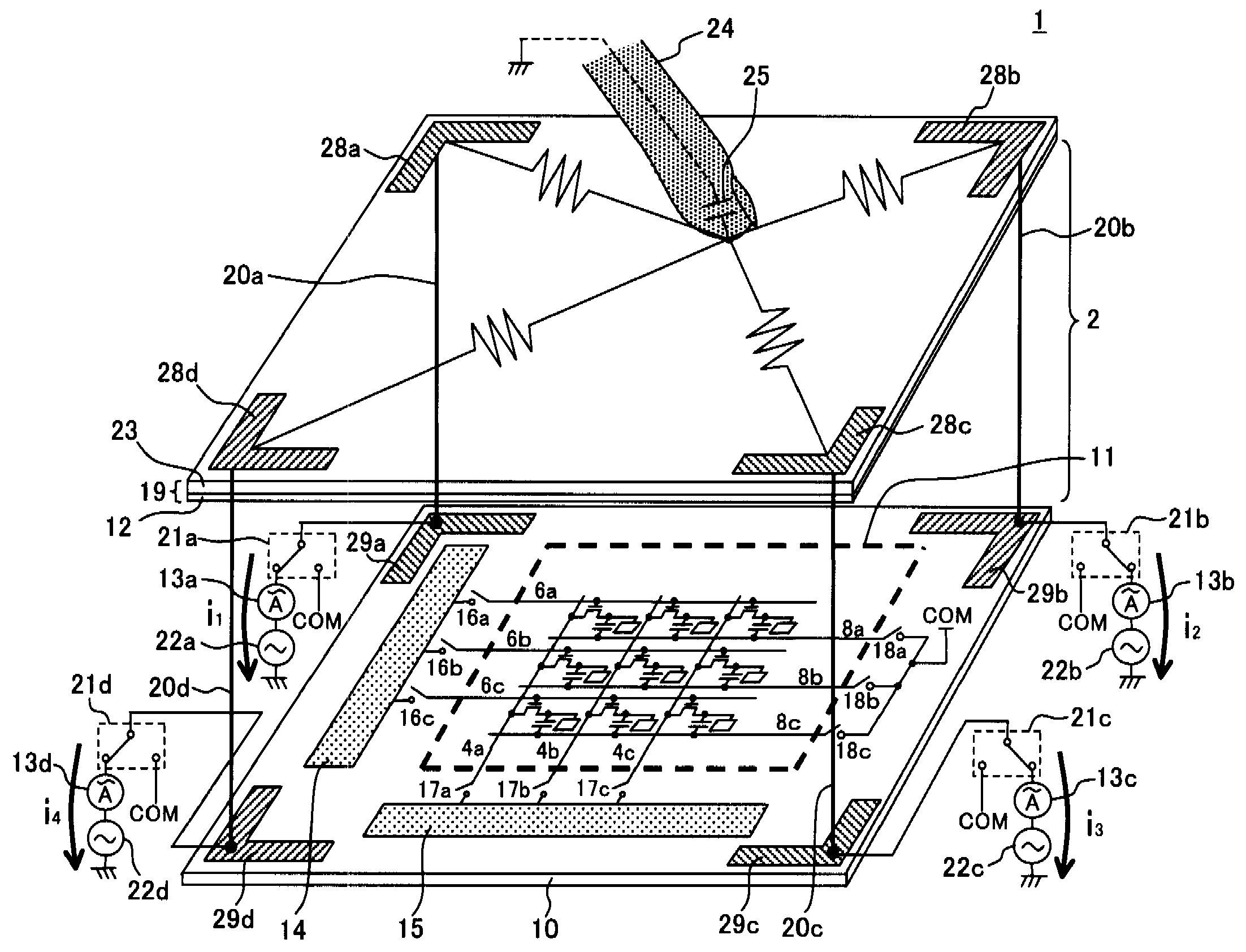
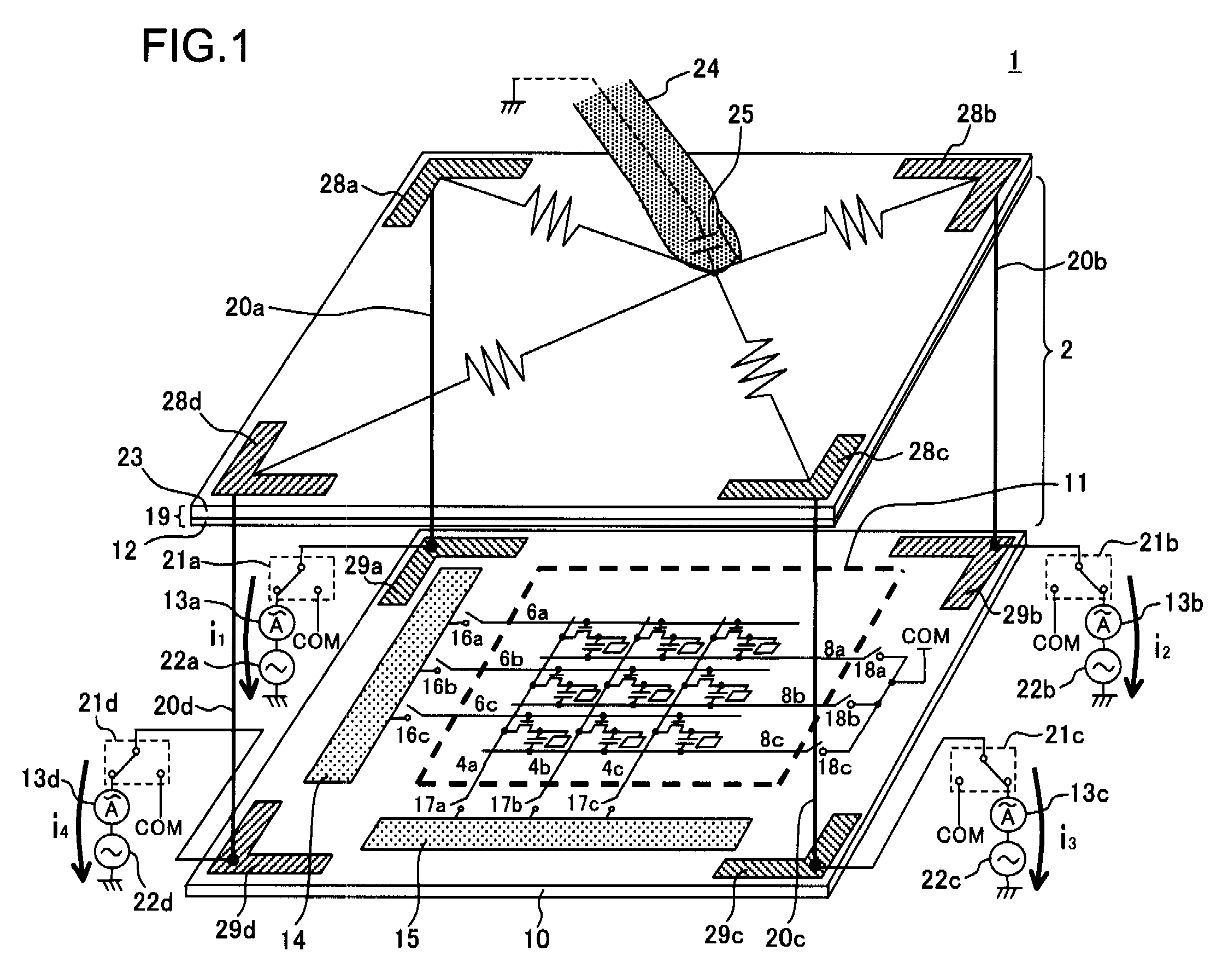
[0069]A flat-panel display device according to a first exemplary embodiment of the present invention will now be described with reference to the drawings, in which FIG. 1 is a perspective view schematically illustrating the structure of a flat-panel display device according to the first exemplary embodiment.

[0070]With reference to FIG. 1, a flat-panel display device 1 is a liquid crystal display (LCD) having a touch sensor capable of sensing whether the surface of the display has been touched by a finger or pen and the coordinates of the touched position. Besides a liquid crystal display, the flat-panel display device 1 can be one such as a plasma display (PDP), organic EL display device or the like. The flat-panel display device 1 has a display device substrate 10, an opposing substrate 19, liquid crystal 2 and a polarizer (not shown).

[0071]The display device substrate 10 is a substrate having a display area 11 in which electrodes for applying electrical signals to the liquid cryst...

second exemplary embodiment

[0123]A display device according to a second exemplary embodiment of the present invention will now be described with reference to the drawings. FIG. 18 is a circuit diagram useful in describing the position detection principle of a display device according to a second exemplary embodiment of the present invention.

[0124]In the first exemplary embodiment, AC voltage is applied directly to the resistor 40 (see FIG. 9). In the second exemplary embodiment, however, an indicating member (e.g., an electronic pen) 30 is connected to AC voltage source 22 and currents i1, i2 that flow via impedance Z are detected by current detecting circuits 13a, 13b, respectively. In this case also the interior and exterior of the display area (which corresponds to area 11 in FIG. 1) are placed at the high impedance in the position detection interval.

[0125]In accordance with the second exemplary embodiment, the parasitic capacitance of the resistor 40 is reduced markedly by placing the interior and exterio...

third exemplary embodiment

[0126]A display device according to a third exemplary embodiment of the present invention will now be described with reference to the drawings. FIG. 19 is a partial sectional view schematically illustrating the structure of a display device according to a third exemplary embodiment of the present invention.

[0127]The display device according to the third exemplary embodiment is an electrophoretic display device (EPD) that utilizes a microcapsule-type electrophoretic element. This is typically a monochromatic EPD active-matrix display. The display device has the opposing substrate 19, an EPD film 50 and the display device substrate 10.

[0128]The opposing substrate 19 includes a transparent plastic substrate 23 such as a polyethylene terephthalate, and an opposing electrode 12, which comprises a transparent conductive film, formed on the inner-side surface of the substrate 23. It should be noted that the opposing substrate 19 may employ a glass substrate instead of the plastic substrate...


PUM


Abstract

A combination flat-panel touch sensor / display device includes a display device substrate on which signal lines, scanning lines and storage capacitance lines for applying electrical signals to liquid crystal are formed. A surface of the flat-panel display device corresponding to a display area has a transparent conductive film serving as an impedance surface. The device further includes current detecting circuits for detecting currents that flow through the impedance surface. In an interval over which the current detecting circuits detect current, at least one of the signal lines, scanning lines and storage capacitance lines is placed at a high impedance. The device reduces thickness without decline in display characteristics.

Description

REFERENCE TO RELATED APPLICATION[0001]This application is based upon and claims the benefit of the priority of Japanese patent application No. 2007-205442, filed on Aug. 07, 2007, the disclosure of which is incorporated herein in its entirety by reference thereto.TECHNICAL FIELD[0002]This invention relates to a flat-panel display device and an electronic apparatus. More particularly, the invention relates to a flat-panel display device having a touch sensor capable of sensing whether the surface of a display has been touched by a finger or pen and the coordinates of the touched position, as well as an electronic apparatus equipped with such a display device.BACKGROUND[0003]A touch sensor, which is a device that detects a position pointed at using a finger or pen, etc., or whether a pointing operation has been performed, is usually used in combination with a flat-panel display device such as an liquid crystal display (LCD) or plasma display (PDP). The output of the touch sensor is in...

Claims


Application Information

Patent Timeline
Patent Type & Authority Applications(United States)
IPC IPC(8): G06F3/045
CPCG06F3/044G06F3/0412G06F3/0418G06F3/0443G06F3/0444
Inventor HAGA, HIROSHI
Owner NEC LCD TECH CORP
Learn More