Device packages

a technology for devices and packaging, applied in the field of device packaging, can solve the problems of low stencil material and processing cost, device not having a planar surface, and stencils that are typically not reuseable, and achieve the effects of reducing the procedure involving fixtures, reducing costs and delays, and easy and precise positioning

Inactive Publication Date: 2009-02-12
AGERE SYST INC
View PDF13 Cites 16 Cited by
  • Summary
  • Abstract
  • Description
  • Claims
  • Application Information

AI Technical Summary

Benefits of technology

[0007]The costs and delays associated with low volume fabrication of electronic devices with ball grids by a procedure involving a fixture is substantially reduced by employing for the fixture a material that is conducive to ablation by lasers having spot power densities in the range 1.2 to 5 watts / sq. mm. In particular, materials such as paper, e.g. paper card stock, and polymers e.g. polyvinyl materials such as Kapton™ (a registered trademark of E.I. DuPont de Nemours Corp.) with thicknesses typically in the range 0.005 to 0.012 inches are advantageously employed. The desired hole pattern having holes with diameters, for example, of 0.014 to 0.016 inches is produced by positioning the impact region of the laser beam using conventional computer control of the laser direction. Thus the point of ablation to form the desired hole is easily and precisely located by such conventional laser beam positioning techniques. For example, a graphical array hole pattern is made with a conventional AutoCAD program that is downloaded to a Markem 612 Platemaker. (This equipment is manufactured by Markem Corporation of Keene, N.H. and includes a sample holder and laser beam positioning component allowing beam position accuracy to ±0.00025 inches.)
[0008]The fixture, in the context of the invention denominated a stencil, is produced by laser ablation in, for example, flexible stock using a laser such as a carbon dioxide laser. Flexible stock is particularly useful in procedures involving devices having a dimension larger than 24 mm. Such devices often do not have a planar surface. A flexible stencil conforms to such non-coplanarity and allows more accurate alignment. In repair of a device a solder paste such as Alpha WS 600 (a paste flux manufactured by Cookson Electronics that includes b-terpiniol, dimethyl propionic acid, non-ionic surfactant, triethanol amine and diethanol amine) is spread over at least the array region of the device. The stencil is then placed on the array region in or on the flux material. The stencil is relatively easily aligned using an optical microscope since during subsequent heating the holes self-align relatively accurately to the desired underlying ball positions through a mechanism resulting from surface tension effects. Solder balls or balls of another conducting material are then spread over the stencil. If the stencil is maintained at a thickness not substantially exceeding the diameter of the ball then only one ball is positioned in each stencil hole. Thus ball placement is easily accomplished. To complete ball attachment the device with its overlying flux stencil and positioned balls is then heated for typical solder ball compositions to a temperature in the range 220 to 235 degrees Celsius. Because such temperatures tend to scorch paper stencils, such stencils are typically not reusable. However, stencil material and processing costs are extremely low relative to typical techniques and so the fabrication of a new stencil for each procedure is not inconvenient and is extremely cost effective. Additionally, since the stencil is easily produced on site, delays associated with outside vendors are eliminated. Additionally stencil replacements as discussed are not a consideration. Thus the invention results in an efficient, reliable, low volume process for ball array fabrication involving nominal associated costs.

Problems solved by technology

Such devices often do not have a planar surface.
Because such temperatures tend to scorch paper stencils, such stencils are typically not reusable.
However, stencil material and processing costs are extremely low relative to typical techniques and so the fabrication of a new stencil for each procedure is not inconvenient and is extremely cost effective.

Method used


Image

  • Device packages
  • Device packages

Examples


example

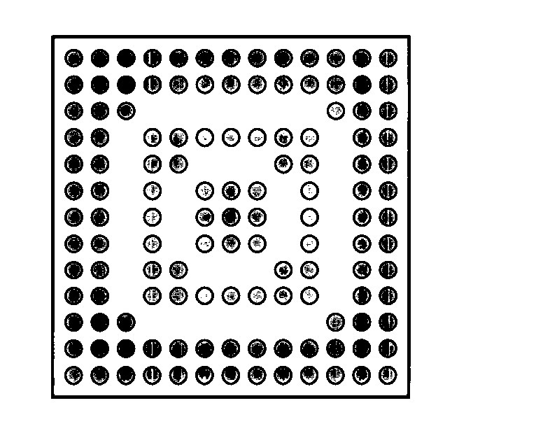
[0021]An AutoCAD 2000 drawing program was employed to produce a representation of the desired array (shown in FIG. 3) for an Agere Systems 225 VTFSBGAB package type with darkened circles representing corresponding stencil holes and lines corresponding to the stencil boundaries. The holes had a diameter of 0.016 inches and the center to center spacing between adjacent holes as shown in FIG. 3 was 0.65 mm. The resulting computer file was loaded onto a floppy disk and then transferred to the host computer (Apple Power Macintosh 8500 computer) for a Markem 612 Platemaker. Using the Adobe Photoshop 3.0 program, the stencil file was loaded into the Photoshop program and subsequently a graphic picture of the stencil loaded in the computer's clipboard. The operating software for the Markem Platemaker was opened and a sample plate file was loaded and then cleared to create a blank image. The stored image of the array pattern on the clipboard was loaded on the plate file using a command denom...


PUM


Abstract

Low volume production of electronic devices having ball attachments, e.g. solder ball arrays, is advantageously achieved using a specific method. In particular a stencil having holes in, for example, the ball grid array pattern is formed by laser ablation of the holes in materials such as paper and polymers. The stencil holes are aligned with corresponding pads on the electronic device. Balls such as solder balls are introduced into the holes and heated to induce adhesion of the balls to the corresponding pads.

Description

TECHNICAL FIELD [0001]This invention related to the packaging of devices and in particular the packaging of devices such as integrated circuits.BACKGROUND OF THE INVENTION [0002]Electronic devices such as integrated circuits and passive electronic devices are packaged in a variety of configurations. One widespread configuration involves the formation of a solder ball array on the exterior of the package to provide electrical communication between the package device and other components such as a printed circuit board or test socket. In such solder ball packaging a series of solder balls are adhered to conductive leads from the packaged device and spatially arranged in an array e.g. a grid of perpendicular rows and columns, with a solder ball at all or some of the column and row intersections.[0003]The formation of such solder bump arrays for mass production i.e. production involving lots greater than 75 individual packages, where 5 to 40 individual packages are ganged together in a ...

Claims


Application Information

Patent Timeline
Patent Type & Authority Applications(United States)
IPC IPC(8): H01L21/768
CPCH05K3/3478H05K2203/107H05K2203/0557H05K2203/041
Inventor HAWKEY, BARRY THOMAS
Owner AGERE SYST INC
Why Eureka
Try Eureka