IC Socket to be Mounted on a Circuit Board

Inactive Publication Date: 2009-02-12
YAMAICHI ELECTRONICS
View PDF31 Cites 12 Cited by
  • Summary
  • Abstract
  • Description
  • Claims
  • Application Information

AI Technical Summary

Benefits of technology

[0020]In the preferred embodiments mentioned above, because the contact is implanted in the resilient member of integral structure, assembling process of the IC socket having the contact mentioned above is simplified. As a result, productivity thereof can be improved and cost reduction thereof can be easily performed.
[0021]The present invention can provide an IC socket corresponding to improvement of the high frequency

Problems solved by technology

Therefore, it is difficult to achieve lowering the inductance to a predetermined level by means of this type of contact.
However, because the number of IC leads increases as the IC becomes highly integrated or highly functionalized, it becomes hard to obtain a uniform contac

Method used


Image

  • IC Socket to be Mounted on a Circuit Board
  • IC Socket to be Mounted on a Circuit Board
  • IC Socket to be Mounted on a Circuit Board

Examples


Example

The First Embodiment

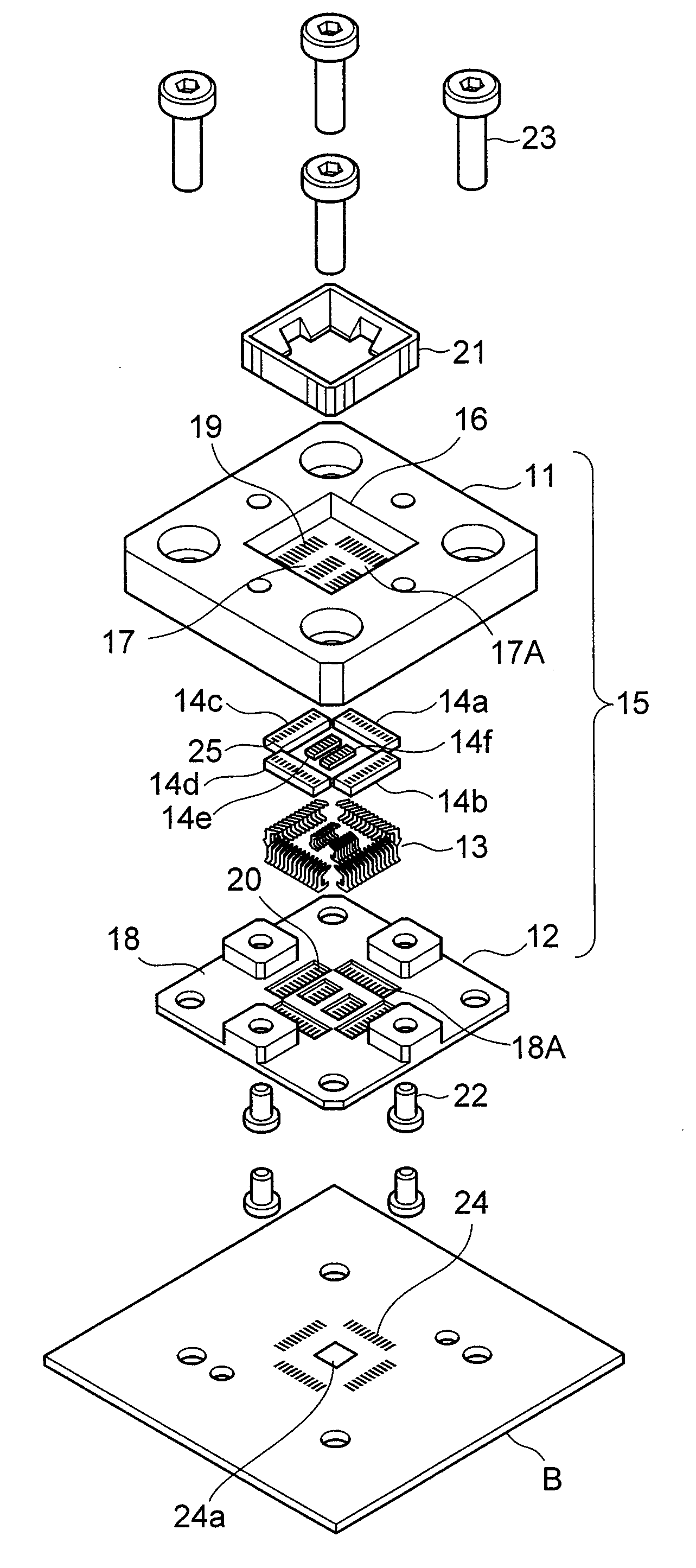
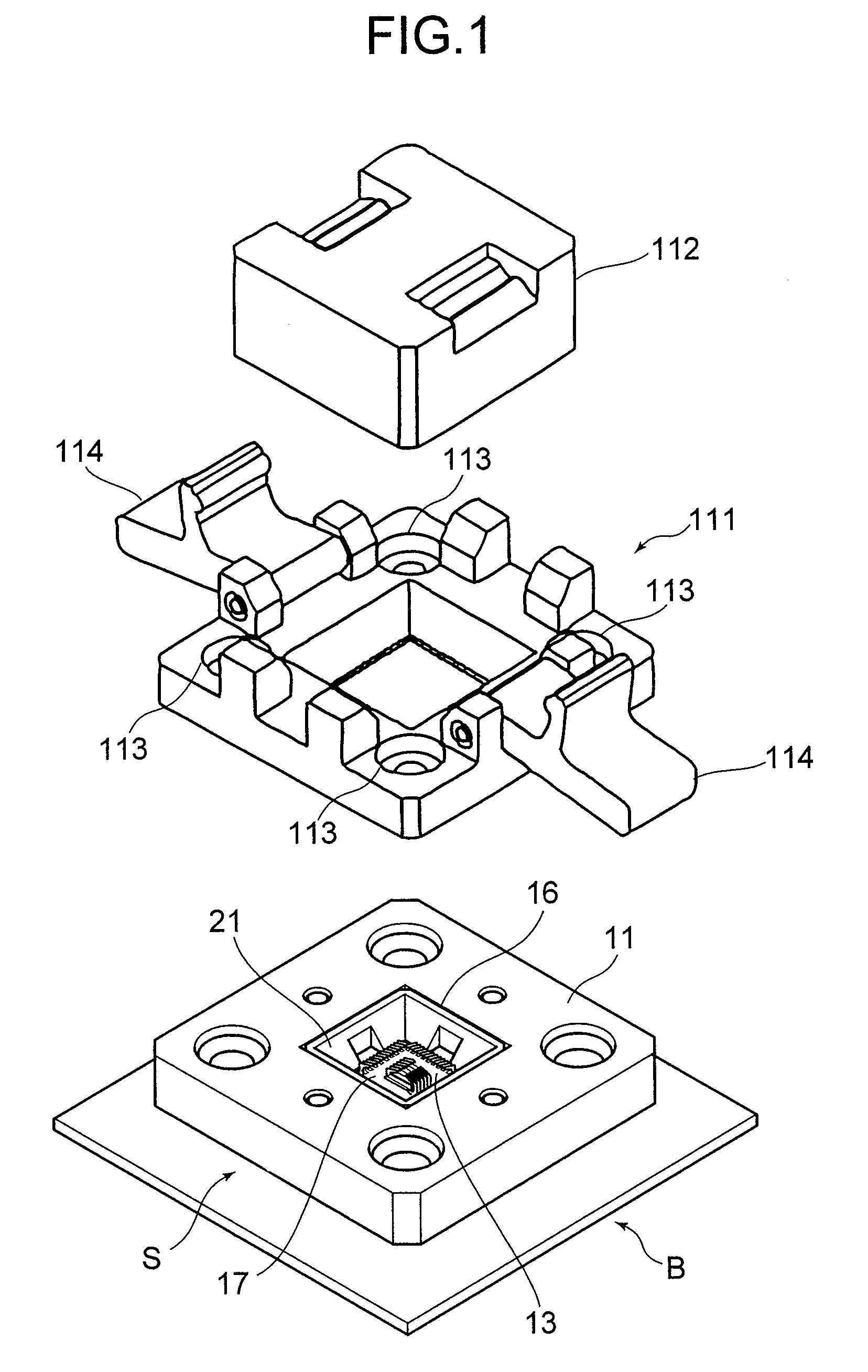
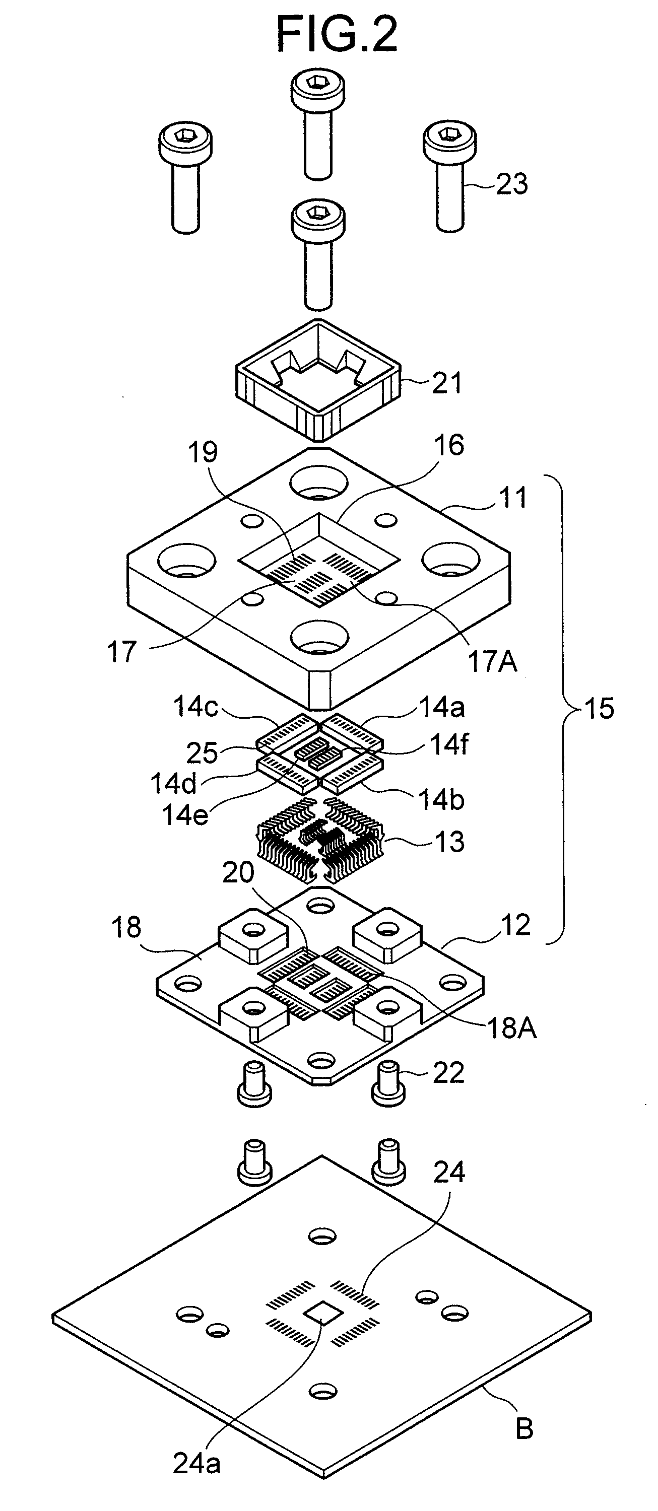
[0038]The IC socket relating to the first embodiment of the present invention will be explained by referring to FIG. 1 to FIG. 8. FIG. 1 is a perspective view showing an example of an IC socket and an IC presser lid mounted on a circuit board such as a test board. FIG. 2 is an exploded perspective view showing the substantial part of the IC socket and the circuit board of the above-mentioned example.

[0039]As shown in FIG. 1 and FIG. 2, the IC socket S is provided with a first assembly 11 of approximately square and a second assembly 12 superimposed on the first assembly 11. These assemblies are formed by molding an insulative synthetic resin having excellent workability. Between the first assembly 11 and the second assembly 12, an insulative resilient member 14 of rubber-elasticity having a plurality of contacts 13 implanted therein is to be inserted. Though the details will be described later, the contact 13 is a rigid structure of metallic material and the resi...

Example

The Second Embodiment

[0074]An IC socket according to the second embodiment of the present invention will be explained referring to FIG. 11 and FIG. 12. An aspect of the IC socket of this embodiment is that each contact is implanted with both sides thereof pinched by two resilient members in the shape of a string or a column extending in the direction of the raw of contacts instead of the resilient member 14 of integral structure explained in the first embodiment. FIG. 11 is a partially magnified cross sectional view showing an example of the IC socket when it is mounted on a circuit board, and FIG. 12 is a partially magnified cross sectional view of the IC socket when an IC is loaded thereon. However, the socket guide 21 is omitted because of simplification.

[0075]As shown in FIG. 11, a first resilient member 31 and a second resilient member 32 are mounted in such a manner as to fit in the resilient member receiving area 27 provided in predetermined positions of the top base board 17...

Example

The Third Embodiment

[0088]An IC socket according to the third embodiment of the present invention will be explained referring to FIG. 13 and FIG. 14. An aspect of the IC socket of this embodiment is that each contact is implanted with both sides thereof pinched by a resilient member in the shape of a string or a column and a jutted synthetic resin extending in the direction of the raw of contacts instead of the integral structure type resilient member 14 explained in the first embodiment. FIG. 13 is a partially magnified cross sectional view showing one example of the IC socket when it is mounted on a circuit board, and FIG. 14 is a partially magnified cross sectional view of a state in which an IC is loaded on the IC socket. However, the socket guide 21 is omitted because of simplification.

[0089]As shown in FIG. 13, a resilient member 36 in the shape of a string is fitted into the resilient member receiving area 35 provided at predetermined places of the top base board 17 of the fi...


PUM


Abstract

The configuration comprises a base board to be mounted a circuit board, with an IC receiving concave place and a resilient member receiving area, having an upper wall and a lower wall surrounding the resilient member receiving area, the upper wall provided with a first slot for contact and the lower wall provided with a second slot, a contact comprising a first contact portion on which a lead of the IC is loaded, a second contact portion coming into contact with a circuit lead of the circuit board, a contact main body communicating the first contact portion with the second contact portion, and a compressing portion protruding from the rear of the contact main body, the resilient member receiving area receiving the resilient member of integral structure, set in the resilient member receiving area, in which a plurality of contacts are implanted, wherein the compressing portion compresses the resilient member in order that a contact pressure can be obtained for the contact to the IC lead and the circuit lead by means of a restoring force of the resilient member.

Description

CROSS-REFERENCE TO RELATED APPLICATIONS[0001]This application is based upon and claims the benefit of priority from the prior Japanese Patent Application No. 2007-207702, filed on Aug. 9, 2007; the entire contents of which are incorporated herein by reference.FIELD OF THE INVENTION[0002]The present invention relates to an IC socket, which acts as a contact medium between a semiconductor integrated circuit (IC) and a circuit board, and more particularly to an IC socket that can favorably correspond to improvement of the high frequency characteristic and miniaturization ofDESCRIPTION OF THE BACKGROUND TECHNOLOGY[0003]Recently, the IC has a plurality of terminals formed on the side or the bottom of the main body thereof, and variety of IC sockets for lowering the inductance of the contact have been developed as the frequency of the operation signal becomes higher and higher. In order to improve the high frequency characteristics for the IC socket by means of realzing a low inductance l...

Claims


Application Information

Patent Timeline
IPC IPC(8): H05K1/00
CPCG01R1/0466
Inventor NAKAMURA, YUJI
Owner YAMAICHI ELECTRONICS
Why Eureka
Try Eureka