Back grinding method for wafer

a back grinding and wafer technology, applied in the direction of grinding machine components, grinding machines, manufacturing tools, etc., can solve the problems of uneven thickness of the base sheet and the pressure sensitive adhesive material, uneven thickness of the wafer as a single body, and difficulty in making uniform wafer thickness with high precision, etc., to achieve uniform thickness, uneven thickness of the wafer, and high precision

Active Publication Date: 2009-02-12
DISCO CORP
View PDF1 Cites 24 Cited by
  • Summary
  • Abstract
  • Description
  • Claims
  • Application Information

AI Technical Summary

Benefits of technology

[0008]Accordingly, it is an object of the present invention to provide a method of grinding a back-side surface of a wafer by which the unevenness of thickness of a wafer as a single body due to the thickness unevenness of a protective member in the prior art can be suppressed and a wafer with a uniform thickness can be obtained in high precision.
[0011]In the present invention, in the wafer angle controlling step the face-side surface of the wafer held by the holding means of the cutting apparatus is controlled to be substantially parallel to the machining plane of the cutting member, whereby it is ensured that when the surface of the resin film is cut in the subsequent resin film cutting step, the cut surface becomes a flat surface parallel to the face-side surface of the wafer. When the resin film has unevenness of thickness, the thickness unevenness is suppressed by cutting the surface of the resin film. When the wafer is held by the holding means of the grinding apparatus with the cut surface of the resin film being directed downward and the back-side surface of the wafer which is exposed in this condition is ground, the ground back-side surface is processed to be a flat surface parallel to the face-side surface of the wafer. In other words, the wafer subjected to back grinding becomes uniform in thickness.
[0013]According to the present invention, instead of using the protective film in the related art which is accompanied by unevenness of thickness, the face-side surface of the wafer is covered with the resin film, the surface of the resin film is cut to form a reference surface parallel to the face-side surface of the wafer, and the surface of the resin film is kept by the holding means of the grinding apparatus, which ensures that the wafer as a single body after the back grinding is uniform in thickness. The resin film after the cutting is a protective member free of thickness unevenness, and its surface serves as an appropriate reference surface in back grinding. Therefore, with the resin film provided on the face-side surface of the wafer, the thickness unevenness of the wafer after the back grinding can be suppressed.
[0014]According to the present invention, the surface of the resin film covering the face-side surface of the wafer is cut to be a flat surface parallel to the face-side surface of the wafer, the surface of the resin film is kept by the holding means of the grinding apparatus, and, in this condition, the back-side surface of the wafer is ground. Therefore, the thickness unevenness of the wafer as a single body due to the thickness unevenness of the protective member in the related art can be suppressed, resulting in that a wafer with a uniform thickness can be obtained in high precision.

Problems solved by technology

In such a protective tape, in many cases, at least one of the base sheet and the pressure sensitive adhesive material has unevenness, if slight, in the thickness thereof.
If such a protective tape is adhered to the face-side surface of the wafer and the back-side surface of the wafer is ground, the unevenness of thickness of the protective tape would be transferred to the wafer, resulting in unevenness of thickness of the wafer as a single body.
If the finished thickness of the wafer is as extremely small as about 30 μm, however, the thickness unevenness of 3 μm is as large as 10% of the wafer thickness and, therefore, it is difficult to make uniform the wafer thickness with high precision.
However, even such a protective film has unevenness of thickness, so that the protective film is not superior to the protective tape from the viewpoint of thickness unevenness.

Method used


Image

  • Back grinding method for wafer
  • Back grinding method for wafer
  • Back grinding method for wafer

Examples


Embodiment Construction

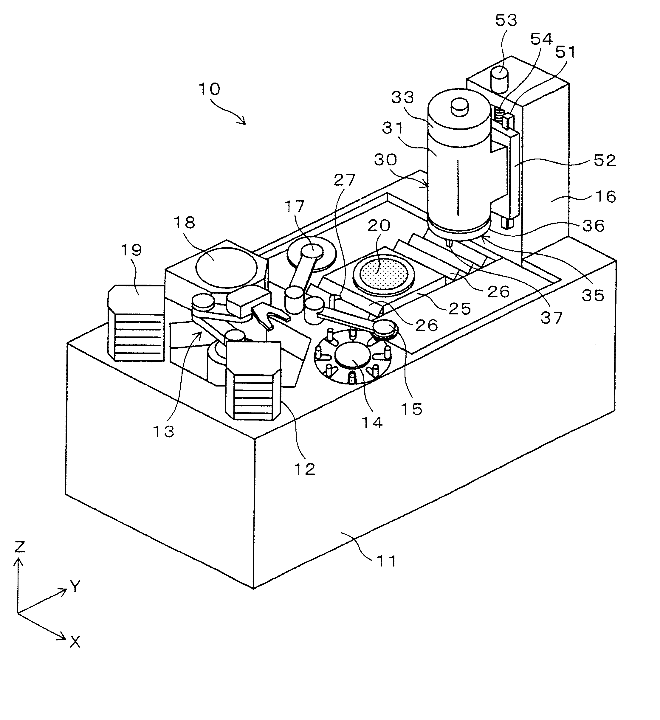
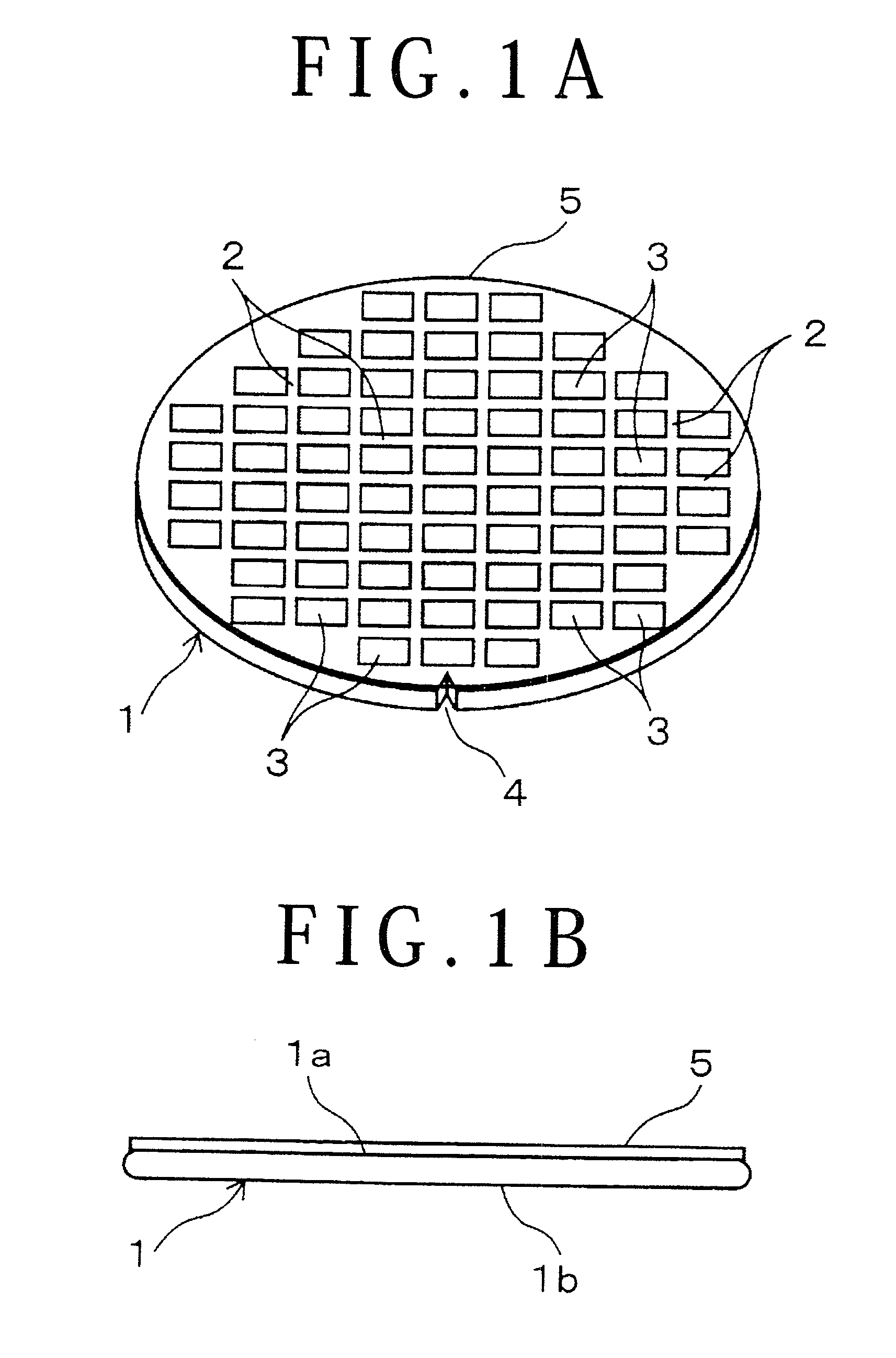
[0028]Now, a method of grinding a back-side surface of a wafer according to an embodiment of the present invention will be described below referring to the drawings. Symbol 1 in FIG. 1 denotes a circular disk-shaped semiconductor wafer (hereinafter referred to as the wafer) to be thinned by back grinding. The wafer 1 is a silicon wafer or the like, and the thickness thereof before machined is, for example, about 700 μm and uniform. A face-side surface 1a of the wafer 1 is demarcated by grid-like planned dividing lines 2 into a plurality of rectangular semiconductor chips (devices) 3. At the surfaces of the semiconductor chips 3, electronic circuits not shown such as ICs and LSIs are formed. In addition, a peripheral surface of the wafer 1 is provided at a predetermined position with a V-shaped notch 4 which indicates the crystal orientation of the semiconductor.

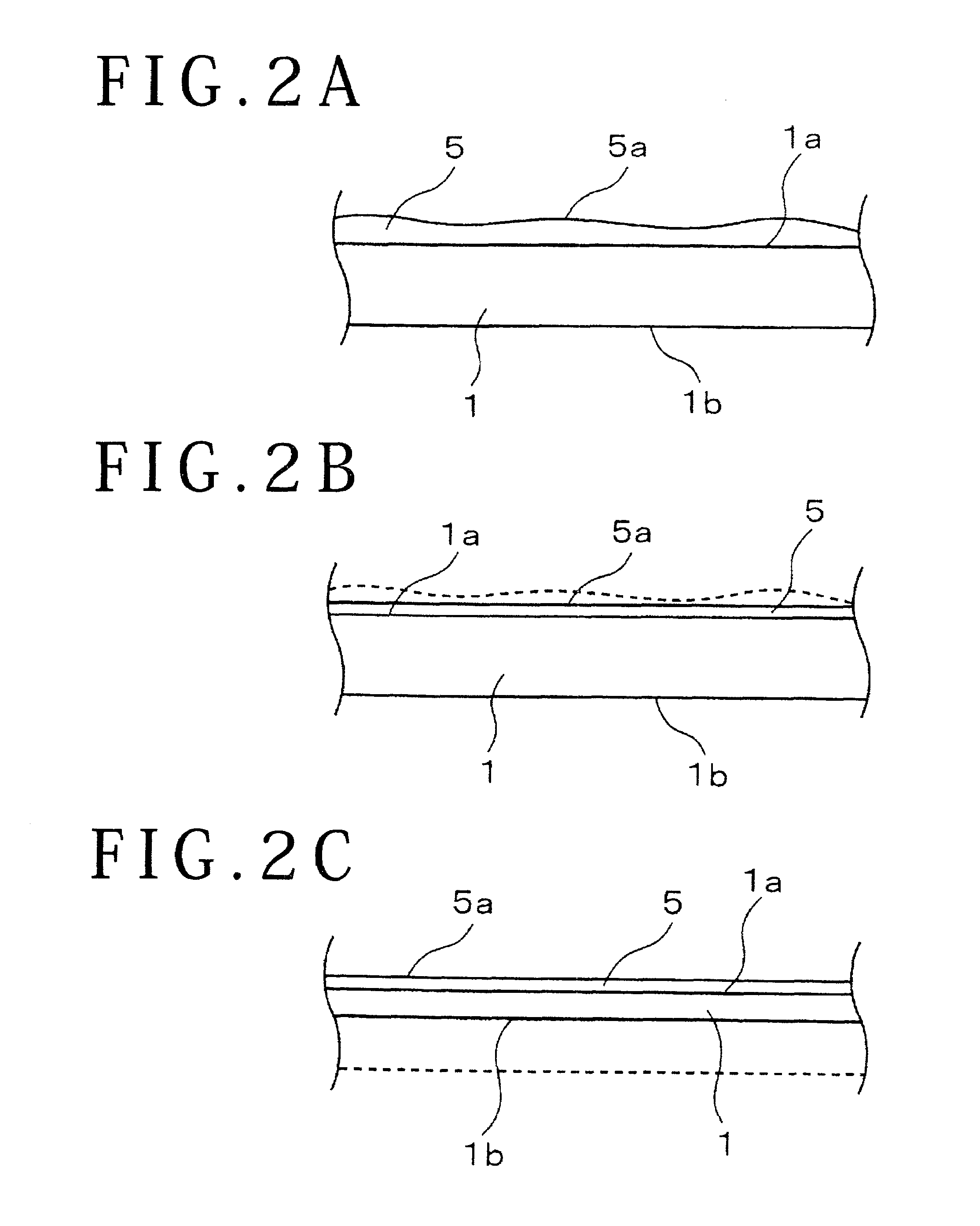
[0029]The method of grinding a back-side surface of a wafer according to this embodiment includes, as shown in FIGS. 2A to ...


PUM

PropertyMeasurementUnit
thicknessaaaaaaaaaa
thicknessaaaaaaaaaa
thicknessaaaaaaaaaa

Abstract

A back grinding method for a wafer includes covering a face-side surface of the wafer with a resin film, and cutting the surface of the resin film to form a flat surface parallel to the face-side surface of the wafer. The wafer is held with the surface of the resin film in contact with a suction surface of a chuck table in a grinding apparatus, and the exposed back-side surface of the wafer is ground. Unevenness in thickness of the resin film is suppressed, whereby the thickness of the wafer subjected to back grinding is made to be uniform.

Description

BACKGROUND OF THE INVENTION[0001]1. Field of the Invention[0002]The present invention relates to a method of grinding a back-side surface of a wafer such as a semiconductor wafer so as to thin the wafer.[0003]2. Description of the Related Art[0004]In a semiconductor device manufacturing process in which a face-side surface of a wafer composed of a semiconductor such as silicon is provided with a multiplicity of devices and the wafer is divided to obtain the devices as individual chips, a step of grinding the back-side surface of the wafer so as to thin the wafer is conducted at the stage of wafer. The thinning of the wafer corresponds to thinning of device packages, and the wafer is thinned, for example, from an initial thickness of around 700 μm to about 200 μm. In accordance with the marked thinning nowadays, the wafers may in some cases be thinned to a very small thickness of 50 μm or 30 μm.[0005]For grinding the back-side surface of a wafer, infeed grinding is generally used in ...

Claims


Application Information

Patent Timeline
Patent Type & Authority Applications(United States)
IPC IPC(8): B24B7/00
CPCB24B7/228
Inventor SEKIYA, KAZUMAKIMURA, YUSUKEMORI, TAKASHIDAII, TOSHIHARU
Owner DISCO CORP
Why Eureka
Try Eureka