X-ray imaging device and method for the manufacturing thereof

a x-ray imaging and solid-state technology, applied in the direction of instruments, electrical appliances, radiation measurement, etc., can solve the problems of mbe, hampered epitaxy of ge on si substrates, and relatively slow process

Active Publication Date: 2009-02-19
CSEM CENT SUISSE DELECTRONIQUE & DE MICROTECHNIQUE SA RECH & DEV +1
View PDF15 Cites 23 Cited by
  • Summary
  • Abstract
  • Description
  • Claims
  • Application Information

AI Technical Summary

Problems solved by technology

As is known in the art, epitaxial growth of Ge on Si substrates is hampered by the substantial difference in lattice parameters of the order of 4%.

Method used


Image

  • X-ray imaging device and method for the manufacturing thereof
  • X-ray imaging device and method for the manufacturing thereof
  • X-ray imaging device and method for the manufacturing thereof

Examples


Embodiment Construction

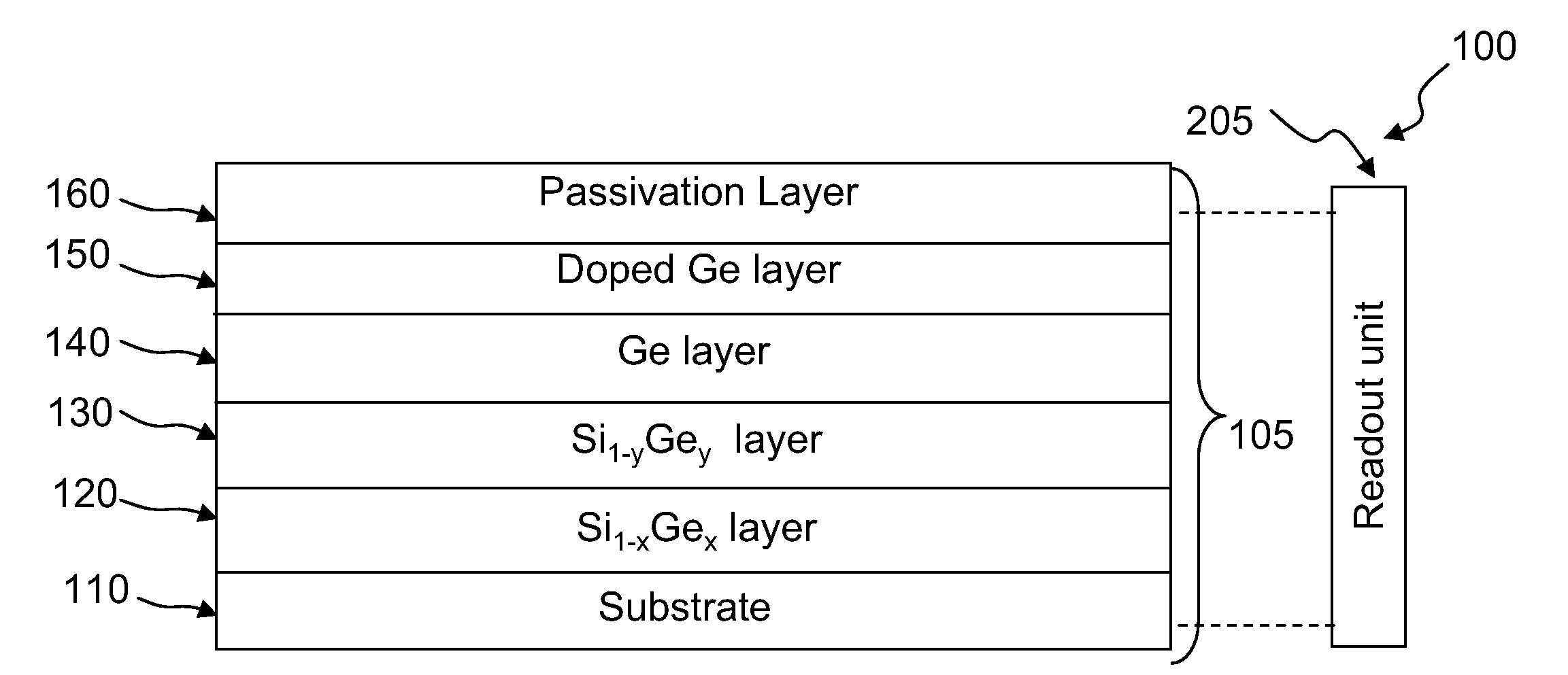
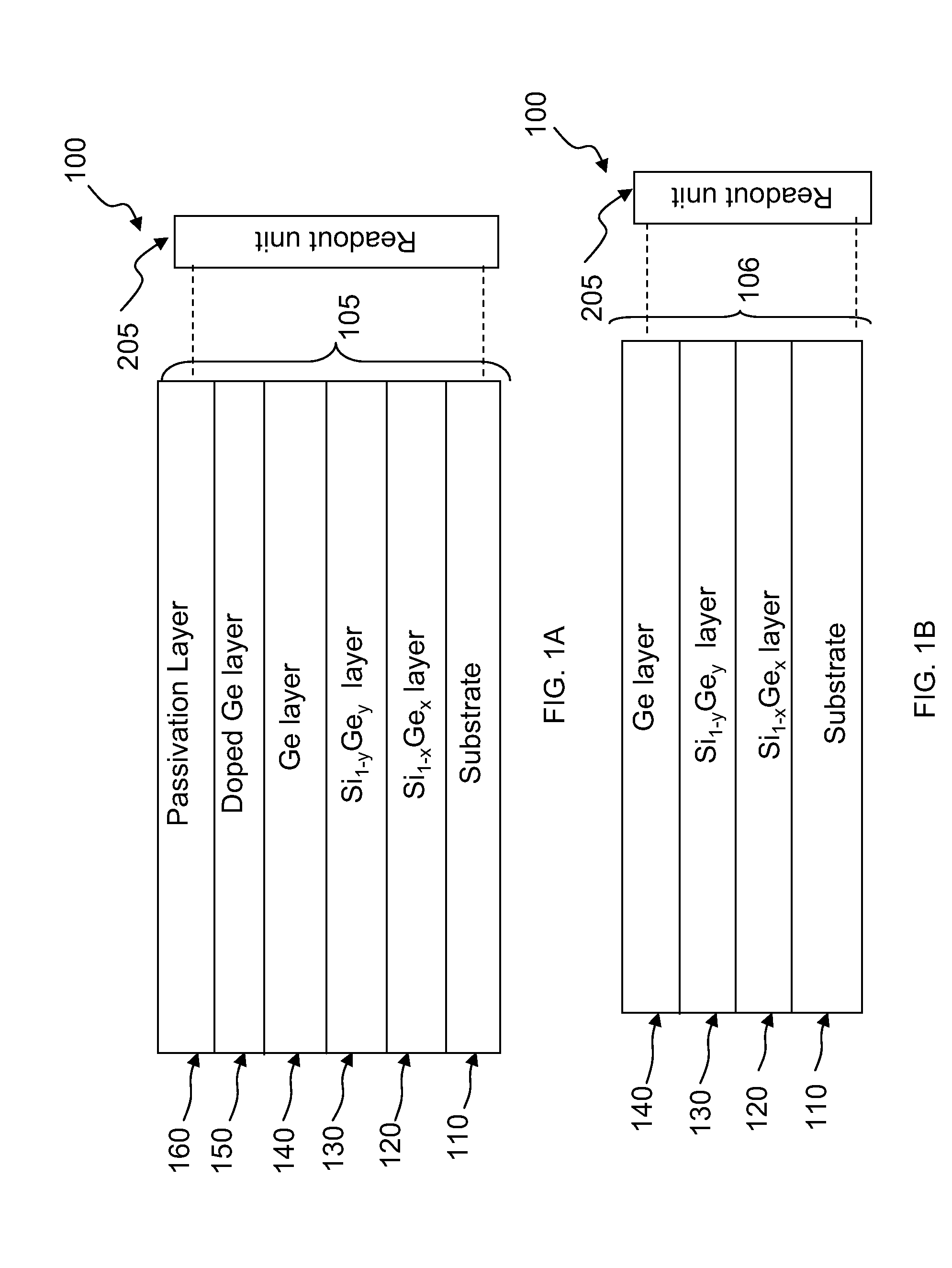
[0035]It is an object of the invention to provide an alternative direct conversion X-ray imaging device and method for manufacturing thereof. It should be noted that the term “direct conversion” refers to any X-ray imaging device that is operable in a scintillator-free manner.

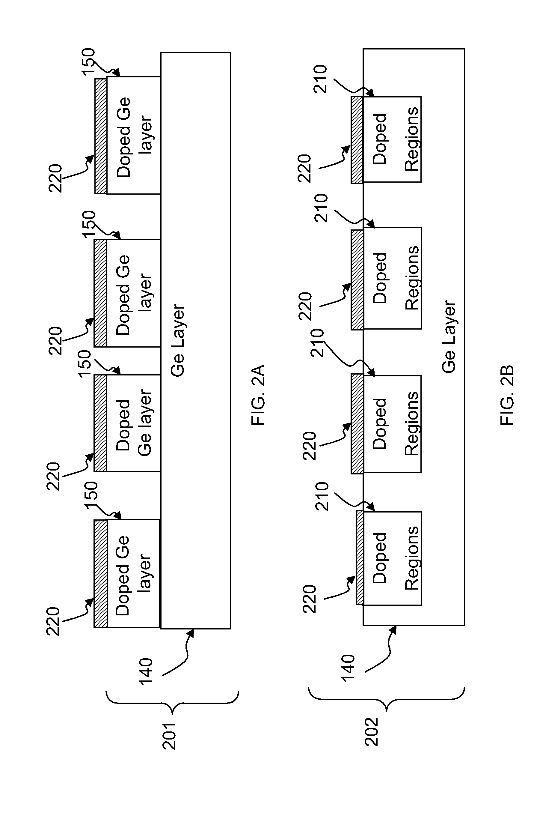
[0036]In embodiments, the X-ray imaging device may include, for example, an X-ray absorber comprising a plurality of semiconductor layers. The plurality of semiconductor layers may include a substrate having a backside; and at least one absorption layer adapted to absorb at least one X-ray photon impinging on the at least one absorption layer that is adapted to correspondingly generate in response to the at least one impinging X-ray photon at least one electron-hole pair; and a readout unit, wherein the readout unit is operatively coupled to the X-ray absorber such to enable readout of the at least one electron-hole pair. More specifically, embodiments of the X-ray imaging device employ pixel elements based on ...


PUM


Abstract

The present invention discloses an X-ray imaging device comprising an X-ray absorber that comprises a plurality of semiconductor layers. The plurality of semiconductor layers comprise a substrate having a backside; and at least one absorption layer adapted to absorb at least one X-ray photon impinging on the at least one absorption layer that is adapted to correspondingly generate in response to the at least one impinging X-ray photon at least one electron-hole pair; and a readout unit, wherein the readout unit is operatively coupled to the X-ray absorber such to enable readout of the at least one electron-hole pair. Additional and alternative embodiments are described and claimed.

Description

CROSS-REFERENCE TO RELATED APPLICATIONS [0001]This patent application claims priority from U.S. Provisional Patent Application No. 60 / 956,391 filed on Aug. 17, 2007, the disclosure of which is incorporated herein by reference in its entirety.FIELD OF THE INVENTION [0002]The invention pertains to imaging devices, and more specifically to solid-state X-ray imaging devices.BACKGROUND OF THE INVENTION [0003]State-of the art digital X-ray imaging devices normally contain a scintillation layer, which converts at least one x-ray photon into visible light, and a photodiode array, which captures the visible image produced by the scintillation layer. Scintillating materials optimised for different X-ray energies are available. Therefore this approach is used for a wide variety of X-ray imaging applications. The efficiency of wavelength conversion in CsI(Tl) for example, a commonly used scintillation material, may be around 10%. This means that per keV of energy of an impinging X-ray photon on...

Claims


Application Information

Patent Timeline
IPC IPC(8): G01T1/24
CPCH01L27/14659H01L31/1812H01L31/028H01L27/14689
Inventor VON KANEL, HANSKAUFMANN, ROLF
Owner CSEM CENT SUISSE DELECTRONIQUE & DE MICROTECHNIQUE SA RECH & DEV
Why Eureka
Try Eureka