Semiconductor device and method of fabricating the same

a technology of semiconductors and semiconductors, applied in the direction of semiconductor devices, transistors, electrical equipment, etc., can solve the problems of reducing the electron mobility in the channel region, the inability to utilize the fabricated mos transistors, and the result of the electric breakdown effect, so as to achieve the effect of effectively controlling the junction depth and reducing the distance between the source region and the drain region

Inactive Publication Date: 2009-02-19
UNITED MICROELECTRONICS CORP
View PDF2 Cites 45 Cited by
  • Summary
  • Abstract
  • Description
  • Claims
  • Application Information

AI Technical Summary

Benefits of technology

[0007]The present invention is directed to a semiconductor device and a method of fabricating the same adapted for effectively reducing the distance between the source region and the drain region, and effectively controlling the depth of the junction between the source region and the drain region.

Problems solved by technology

Hence, an electrical breakdown effect is resulted due to the abundant generation of carriers in the channel near the drain region.
Otherwise, the MOS transistor fabricated cannot be utilized.
Consequently, the electron mobility in the channel region is decreased and the operating speed of the device is reduced, increasing the power consumption.
Nevertheless, it is harder to effectively control the depth and the width of a recess formed by a single-step etching process.
Therefore, a transistor fabricated using the single-step etching process may result in undesired problems such as a distance between the source region and the drain region that is too long or a depth of the junction between the source contact region and the drain contact region that is too deep.

Method used


Image

  • Semiconductor device and method of fabricating the same
  • Semiconductor device and method of fabricating the same
  • Semiconductor device and method of fabricating the same

Examples


Embodiment Construction

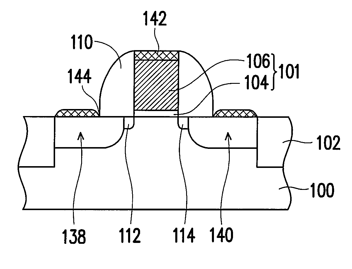
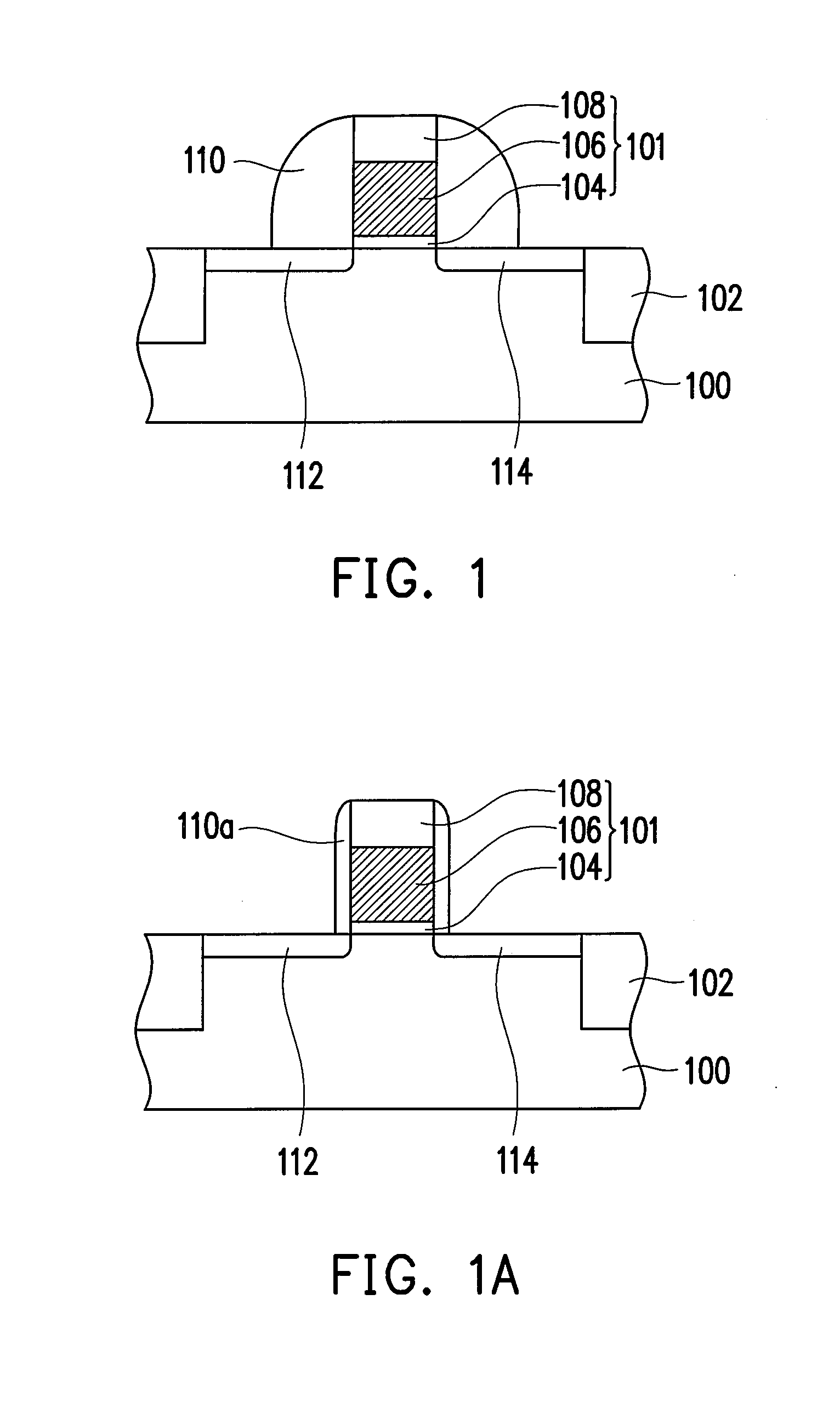
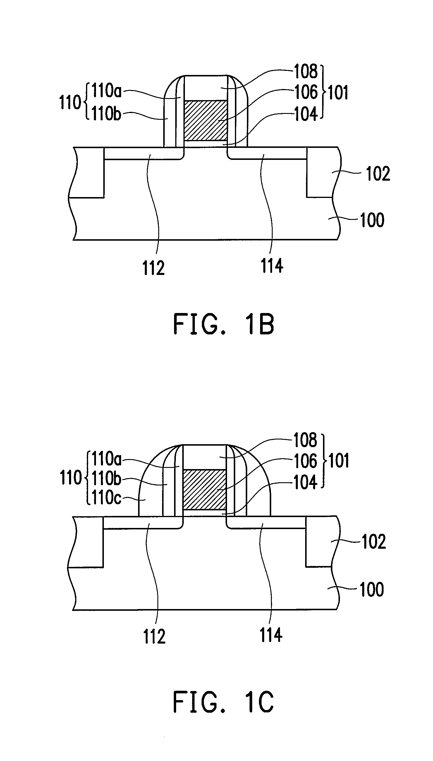
[0046]Referring to FIG. 1, a substrate 100 is provided. The substrate 100 may be, for example, a bulk-Si substrate or a silicon-on-insulator (SOI) substrate. In an embodiment, the substrate 100 includes P-type silicon. In an embodiment, a well region, such as an N-type well and / or a P-type well (not shown), is formed in the substrate 100. Next, an isolation structure 102 is formed in the substrate 100. The method for forming the isolation structure is, for example, a shallow trench isolation (STI) process.

[0047]Next, a gate structure 101 is formed on the substrate 100. The gate structure 101 includes a patterned gate dielectric layer 104, a patterned gate conductor layer 106, a patterned cap layer 108, and a spacer 110. The material of the gate dielectric layer 104 is, for example, silicon oxide, and the method of forming the gate dielectric layer 104 is, for example, a thermal oxidation process. The material of the gate conductor layer 106 includes a silicon-based material such as ...


PUM


Abstract

A method of fabricating a semiconductor device is provided. The method includes forming a gate structure on a substrate. The gate structure includes a patterned gate dielectric layer, a patterned gate conductor layer, a cap layer and a spacer. Next, a first and a second recesses are formed in the substrate on the two sides of the gate structure. Thereafter, a protection layer is formed on the bottom surfaces of the first and the second recesses, and then a etching process is performed to laterally enlarge first and the second recesses towards the direction of the gate structure. Thereafter, a material layer is respectively formed in the first recess and the second recess. Afterward, two source/drain contact regions are respectively formed in the material layers of the first recess and the second recess.

Description

BACKGROUND OF THE INVENTION[0001]1. Field of the Invention[0002]The present invention relates to an integrated circuit and a method of fabricating the same, and more particularly, to a semiconductor device and a method of fabricating the same.[0003]2. Description of Related Art[0004]A metal-oxide semiconductor (MOS) transistor is a basic structure extensively adopted by a variety of semiconductor devices such as memory devices, image sensors, or display devices. A typical MOS transistor includes a silicon dioxide dielectric layer, a gate conductor layer, and a heavily doped source / drain contact region. The size of a semiconductor device is reduced as the line width of the semiconductor device is reduced. As a result, the width of the gate in a conventional MOS transistor and the channel length within the MOS transistor are also reduced. Since the threshold voltage is decreased and the sub-threshold current is increased, a short channel effect is resulted. On the other hand, as the g...

Claims


Application Information

Patent Timeline
Patent Type & Authority Applications(United States)
IPC IPC(8): H01L31/0312H01L21/336H01L29/76
CPCH01L21/30608H01L21/3065H01L21/3083H01L21/3085H01L29/165H01L29/7848H01L29/6656H01L29/6659H01L29/66628H01L29/66636H01L29/7833H01L29/665
Inventor CHEN, HSUAN-HSUCHEN, HSIN-CHILIAO, JIUNN-HSIUNG
Owner UNITED MICROELECTRONICS CORP
Why Eureka
Try Eureka