Semiconductor memory device and control method thereof
a memory device and semiconductor technology, applied in the field of semiconductor memory, can solve the problems of increasing leakage current and physical presence of defective memory cells
- Summary
- Abstract
- Description
- Claims
- Application Information
AI Technical Summary
Benefits of technology
Problems solved by technology
Method used
Image

Examples
first embodiment
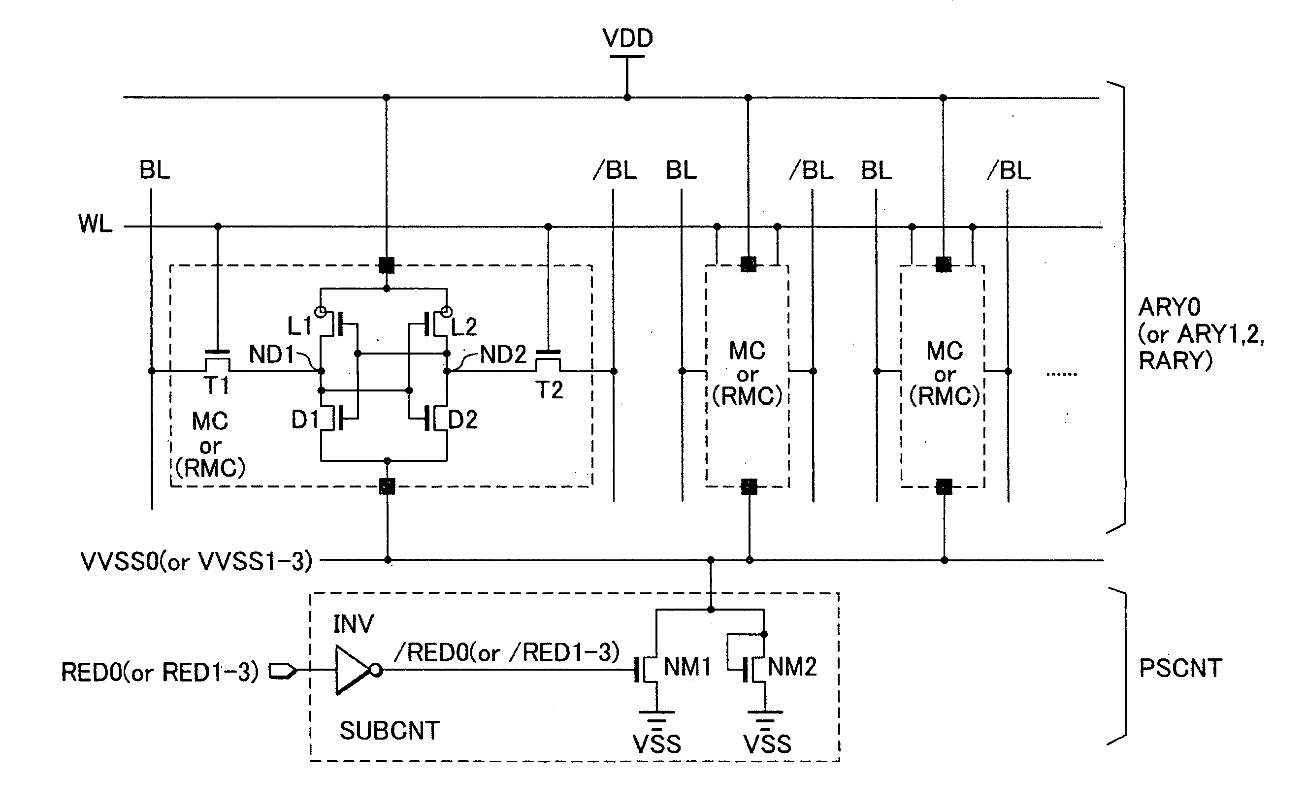
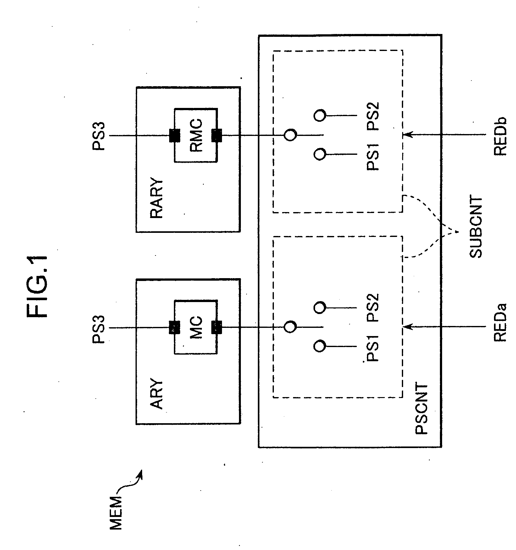
[0034]FIG. 1 shows a A semiconductor memory MEM includes a regular cell array ARY having a plurality of regular memory cells MC, a redundant cell array RARY having a plurality of redundant memory cells RMC and a power supply control circuit PSCNT. The power supply control circuit PSCNT supplies the regular cell array ARY and the redundant cell array RARY with a first power supply voltage PS1 or a second power supply voltage PS2. The plurality of redundant memory cells RMC are used, instead of defective regular memory cells in the regular cell array ARY. Note that, in some cases, the semiconductor MEM includes more than one regular cell array ARY.
[0035]In addition, the regular cell array ARY is not limited to the regular cell array ARY shown in FIG. 1. It is possible that the regular cell array ARY comprises the single regular memory cell MC. It is also possible that the regular cell array ARY comprises the plurality of regular memory cells MC coupled to a single bit line.
[0036]The ...
third embodiment
[0071]FIG. 6 shows an operation of the Circles in FIG. 6 indicate that there is no defect in the regular cell array ARY or in the redundant cell array RARY. A triangle in FIG. 6 indicates that the redundant cell array RARY is handled as the pseudo defective cell array. An X in FIG. 6 indicates the defective regular cell array ARY.
[0072]If there is no defective regular memory cell in the regular cell array ARY (non-redundant time), the redundant signal RED3 is set at the H level. In the power supply control circuit PSCNT in FIG. 4, the nMOS transistor NM1 corresponding to the regular cell arrays ARY0 through ARY2 is switched on, and the nMOS transistor NM1 corresponding to the redundant cell array RARY is switched off. The virtual ground lines VVSS0 through VVSS2 are set to the ground voltage VSS (a first power supply voltage) and the virtual ground line VVSS3 is set to a voltage VSS+α (a second power supply voltage). The α indicates a threshold voltage of the nMOS transistor NM2.
[0...
fourth embodiment
[0082]In the fourth embodiment, if there is no defective regular memory cell in the regular cell array ARY (non-redundant time), the pMOS transistor PM1 corresponding to the regular cell arrays ARY0 through ARY2 is switched on and the pMOS transistor PM1 corresponding to the redundant cell array RARY is switched off. The virtual power supply lines VVDD0 through VVDD2 are set to the ground voltage VDD (a first power supply voltage) and the virtual power supply line VVDD3 is set to a voltage VSS−α (a second power supply voltage).
[0083]A decrease in the power supply voltage supplied to the unused redundant cell array RARY causes a decrease in difference between the power supply voltage and the ground voltage VSS (a third power supply voltage) in the redundant memory cells RMC in the redundant cell array RARY. For example, if the power supply voltage is one point two (1.2) V and the threshold voltage of the pMOS transistor PM2 is minus zero point five (−0.5) V, the virtual power supply ...
PUM
 Abstract
Description
Claims
Application Information
 - R&D
- Intellectual Property
- Life Sciences
- Materials
- Tech Scout
- Unparalleled Data Quality
- Higher Quality Content
- 60% Fewer Hallucinations
Browse by: Latest US Patents, China's latest patents, Technical Efficacy Thesaurus, Application Domain, Technology Topic, Popular Technical Reports.
© 2025 PatSnap. All rights reserved.Legal|Privacy policy|Modern Slavery Act Transparency Statement|Sitemap|About US| Contact US: help@patsnap.com