Nonvolatile memory device, system, and method providing fast program and read operations

a nonvolatile memory and program operation technology, applied in the field of semiconductor memory devices, can solve the problems of mroms, proms, eproms not allowing the immediate update of stored data, and lose stored data in the absence of applied power, so as to prevent reliability degradation and increase the programming rate

Active Publication Date: 2009-02-19
SAMSUNG ELECTRONICS CO LTD
View PDF19 Cites 61 Cited by
  • Summary
  • Abstract
  • Description
  • Claims
  • Application Information

AI Technical Summary

Benefits of technology

[0008]Accordingly, embodiments of the invention enjoy an increased programming rate while preventing

Problems solved by technology

Volatile semiconductor memory devices are generally characterized by high speed read and write operations, but lose stored data in the absence of app

Method used


Image

  • Nonvolatile memory device, system, and method providing fast program and read operations
  • Nonvolatile memory device, system, and method providing fast program and read operations
  • Nonvolatile memory device, system, and method providing fast program and read operations

Examples


Embodiment Construction

[0030]Embodiments of the invention will be described below in the context of a NAND-type flash memory device as examples illustrating structural and operational features by the invention.

[0031]The present invention may, however, be embodied in different forms and should not be constructed as being limited to only the illustrated embodiments. Rather, these embodiments are provided as teaching examples.

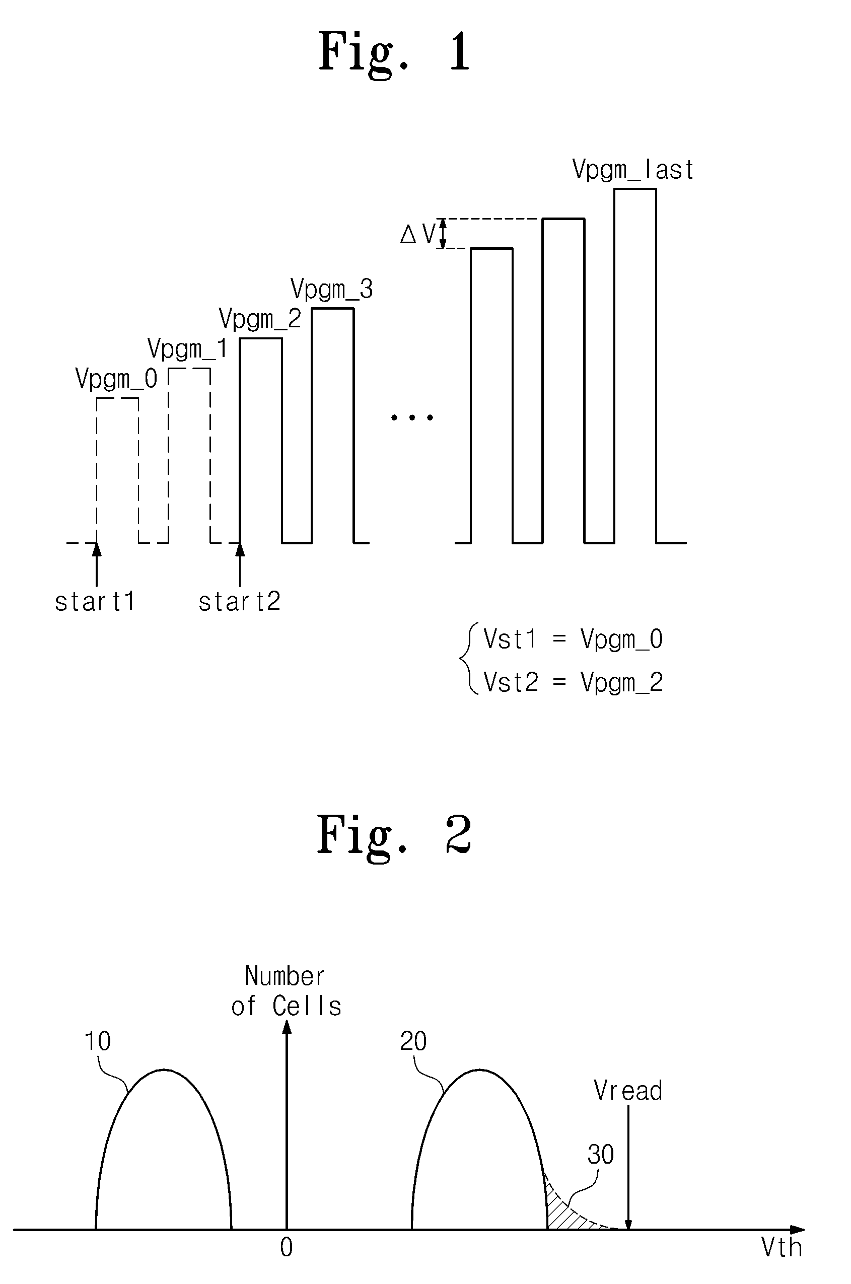
[0032]FIG. 1 is a waveform diagram of a program start voltage according to an embodiment of the invention. Referring to FIG. 1, in a programming operation, a program voltage Vpgm applied to a word line of a memory cell is increased by a step voltage ΔV for each incremental programming loop. The program voltage Vpgm is raised gradually until a last program voltage Vpgm_last is applied to the memory cell during a last programming loop.

[0033]To increase the overall programming rate for a constituent flash memory device, it is necessary to decrease the number of programming loops. Hence, th...


PUM


Abstract

Disclosed are program and read methods for a nonvolatile memory system, including determining to program first data in which one of fast and normal modes; providing the first data with an error code generated by a multi-bit ECC engine, in the fast mode, and generating second data; programming the second data in a cell array by a program voltage having a second start level higher than a first start level; and reading the second data from the cell array, the second data being output after processed by the multi-bit ECC engine that detects and corrects an error from the second data.

Description

CROSS-REFERENCE TO RELATED APPLICATIONS[0001]This U.S. non-provisional patent application claims priority under 35 U.S.C. § 119 to Korean Patent Application No. 10-2007-82330 filed on Aug. 16, 2007, the subject matter of which is hereby incorporated by reference.BACKGROUND[0002]The present invention relates generally to semiconductor memory devices, and more particularly to a nonvolatile memory devices, systems and method of performing read and program operations.[0003]Semiconductor memory devices may be classified as volatile and nonvolatile in the operative nature. Volatile semiconductor memory devices are generally characterized by high speed read and write operations, but lose stored data in the absence of applied power. In contrast, nonvolatile semiconductor memory devices retain stored data in the absence of applied power. Thus, the nonvolatile semiconductor devices are widely used in applications requiring data retention regardless of power supply state. There are many kinds ...

Claims


Application Information

Patent Timeline
IPC IPC(8): H03M13/05G06F11/10
CPCG06F11/1072G11C11/5628G11C11/5642G11C16/0483H03M13/6306G11C2211/5641H03M13/098H03M13/13H03M13/356G11C29/00G11C16/00
Inventor JO, SUNG-KYUYIM, YONG-TAE
Owner SAMSUNG ELECTRONICS CO LTD
Why Eureka
Try Eureka