It is well known that surface defects appear during manufacturing of semiconducting substrates such as SOI (
Silicon On Insulator) substrates intended specifically for micro-electronic, optoelectronic application, etc.
During these heat treatments, the substrate is subjected to temperature gradients and a plastic deformation that causes the appearance of surface defects called Slip lines on the
active layer that reduce the substrate quality.
For example, high quality SOI type substrates require heat treatments at a temperature of 1100° C. or even more than 1200° C., causing the formation of slip lines, particularly close to contact zones between the substrate and the support holding the substrate in position during heat treatments.
The slip lines will deteriorate the quality of the
monocrystalline silicon on insulator layer and consequently electronic components that are made later.
Fast and reliable detection of all slip lines using a single detection technique is found to be very difficult.
If several techniques commonly used in industry are used and the results are compared, it can be seen that there is no technique capable of identifying all slip lines and in particular slip lines that occur at the periphery of the substrate.
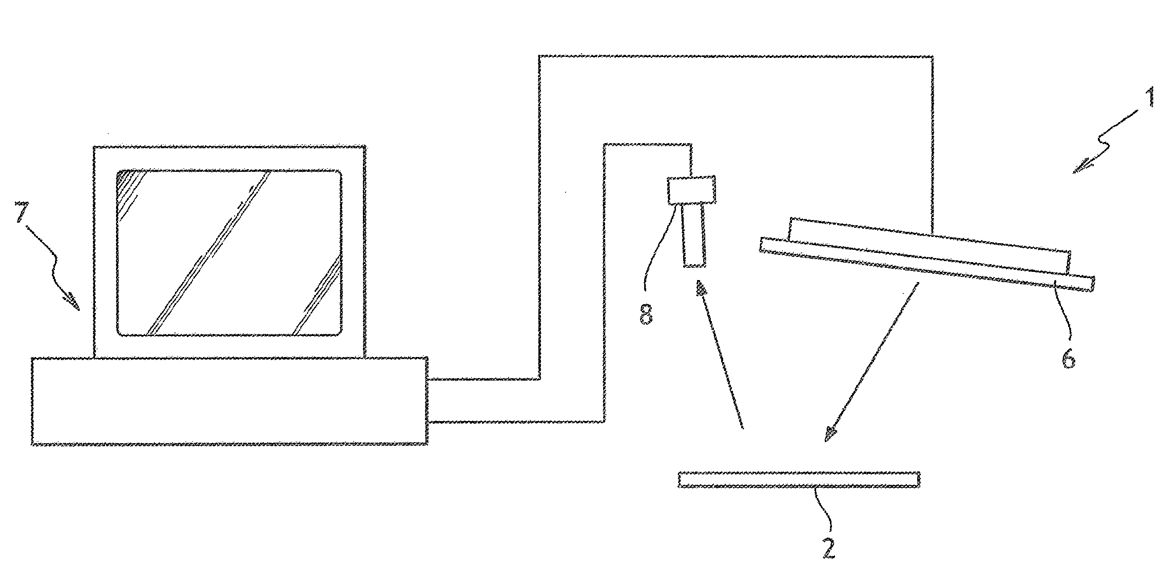
Techniques based on detection of beams of reflected and / or
scattered light at the surface of the substrate cannot be used around the edge of the substrate where the
wafer has a rounded edge such that light cannot be collected and therefore the measurement cannot be made.
There are powerful and complex laboratory devices that admittedly are capable of detecting practically all defects that can be detected optically, such as slip lines or holes present at the surface, etc.
However, these devices are very expensive and substrates can only be analyzed at a rate of about 7 substrates per hour.
These methods have the
disadvantage that they require a particularly long development time and their efficiency is not good.
These methods are incapable of detecting low amplitude slip lines.
In particular, these methods are incapable of detecting slip lines present on the edges of the substrate (the rounded edges make it impossible to satisfactorily collect reflected light), although slip lines are particularly frequent at edges.
This method has the
disadvantage firstly that it can only be used to detect large slip lines, and secondly, that the
processing time for a substrate according to this method is long and results in a limited supply rate of analysed substrates.
This method presents the disadvantage to be inefficient to detect small defects too.
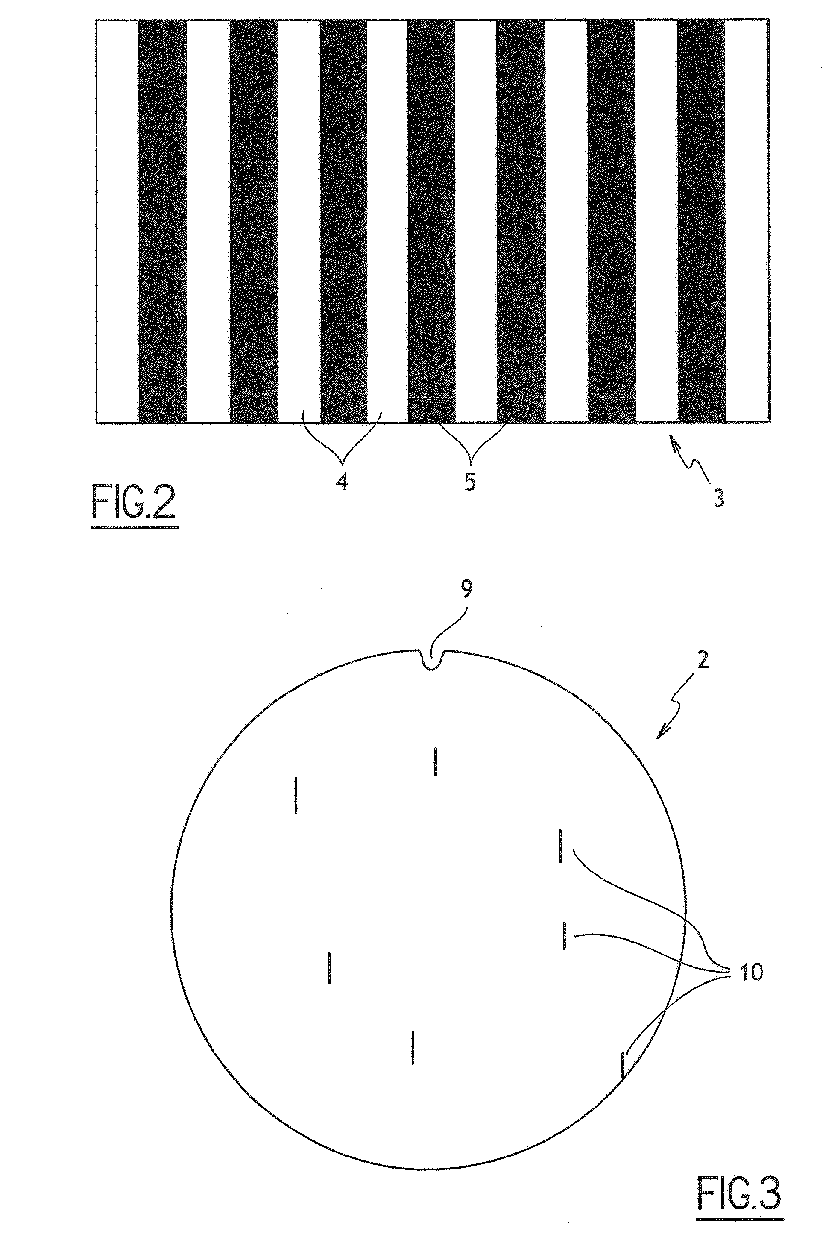
Moreover, not all these methods can efficiently detect so-called non-transferred zones that can occur during a manufacturing process comprising a step to transfer a layer and then a step to detach the layer using SmartCut™ process.
ZNT zones at the edge of the substrate are not always detected, particularly in a zone in which measurements cannot be made due to the rounded edge of the substrate.
It is also found that above a given size, these techniques are not very effective at detecting ZNT zones.

