

Conductive connecting pin and package substrate
a technology of connecting pins and substrates, which is applied in the direction of non-metallic protective coating applications, transportation and packaging, and the improvement of the adhesion of the insulation substrate, etc., can solve the problems that the separation of the conductive connecting pin cannot be prevented, and achieve the prevention of cracks and breakages of the conductor circuit or the like which holds the projecting pin, and the concentration of stress on the projecting pin can be relaxed. , the effect of large joining area
- Summary
- Abstract
- Description
- Claims
- Application Information
AI Technical Summary
Benefits of technology
Problems solved by technology
Method used
Image

Examples
first embodiment
[0196]Referring to FIGS. 1 to 8, a package substrate according to a first embodiment will now be described together with a method of manufacturing a build-up substrate. Although the following method is performed by a semi-additive method, a full additive method may be employed.
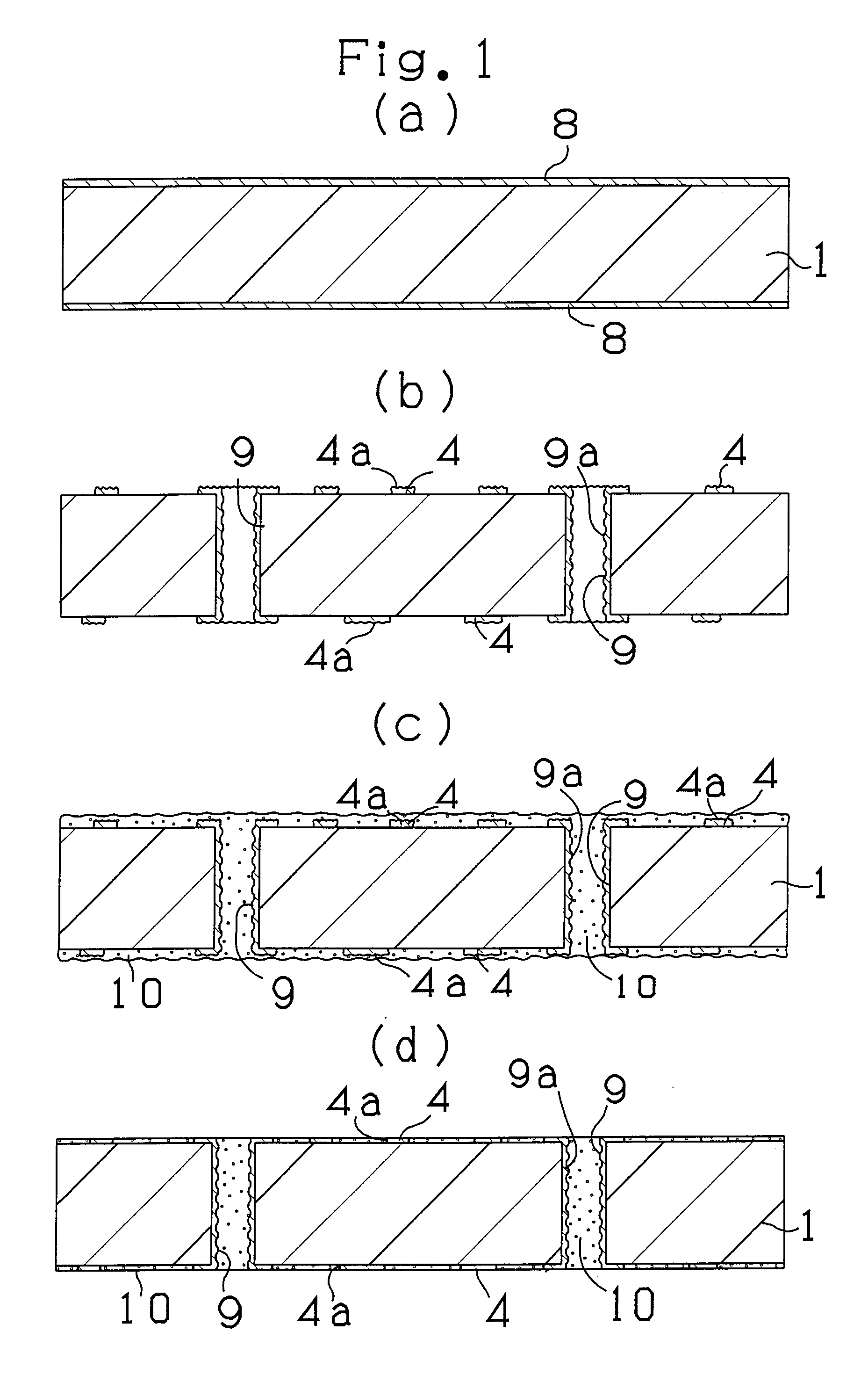
[0197](1) Initially, a core substrate having a conductive layer formed on the surface thereof is manufactured. The core substrate may be a copper-clad laminated pad incorporating a resin insulating substrate, such as a glass epoxy substrate, a polyimide substrate or a bismaleimide-triazine resin substrate which has two surfaces to each of which copper foil 8 has been bonded (refer to FIG. 1 (a)). The copper foil 8 has either side formed into a coarsened surface (a mat surface) so as to be made to firmly contact with the resin substrate. A through hole is formed in the substrate by drilling, and then electroless plating is performed so that a through hole 9 is formed. It is preferable that the electroless plati...
example 4
d. Example 4
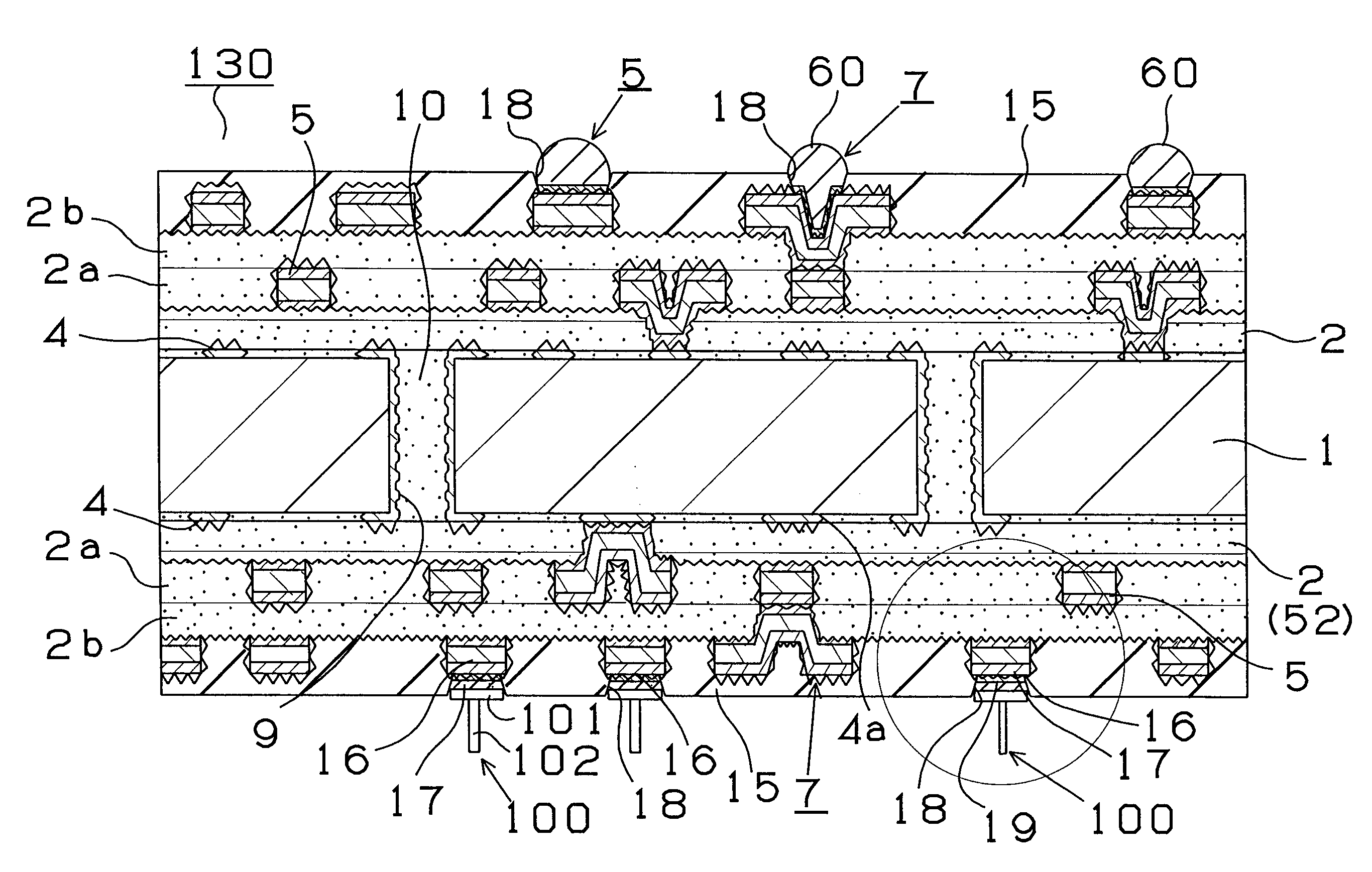
[0277]The basic structure is the same as that according to example 2 described with reference to FIG. 12. A package substrate 135 (see FIG. 14) has a structure that a plurality of via holes 7 formed in a circular configuration are as well as provided for the inter layer resin insulating layer 52 which is the inner layer. Moreover, the outer via hole 7 provided with the pad 16 and the inner via hole 7 are joined to each other. The package substrate 135 has the structure that the plurality of the via holes 7 are joined to one another. Thus, peeling off the pad 16 can significantly be prevented.
[0278]As described above, it is preferable that each of the modifications has the structure that the inner conductor layer with which the pad is provided is provided for the core substrate 1. The conductor layer on the core substrate is made to firmly contact with the insulating substrate which is the core substrate through the coarsened surface (the mat surface). When connection wit...
second embodiment
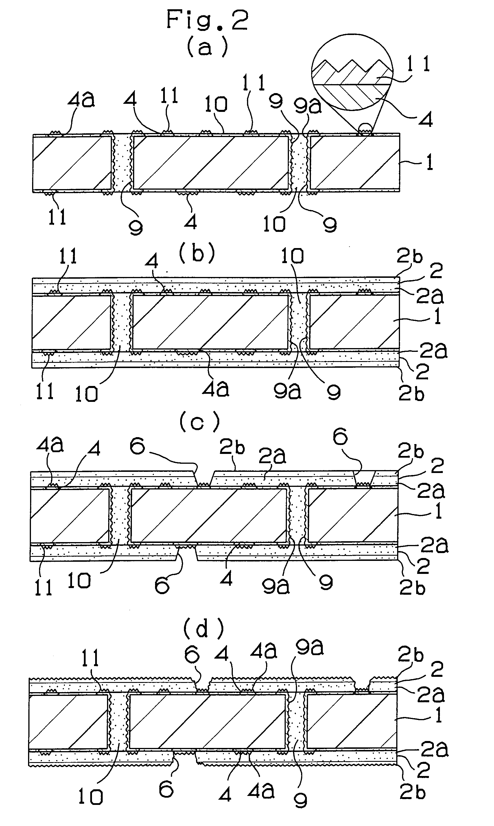
[0286]A package substrate according to a second embodiment and a manufacturing method therefor will now be described. The foregoing steps (1) to (13) are similar to those according to the first embodiment described with reference to FIGS. 1 to 5. Therefore, the similar steps are omitted from illustration and description.
(14) The conductor layer 5 and the coarsened layer 11 of the build-up substrate obtained in steps in (1) to (13) and shown in FIG. 5 are formed. Then, covering with the organic resin insulating layer 15 having the opening 18 through which the pad 16 is exposed is performed (see FIG. 19). It is preferable that the thickness of the organic resin insulating layer is 5 μm to 40 μm. If the thickness is too small, the insulating performance deteriorates. If the thickness is too large, opening cannot be easily formed. What is worse, undesirable contact with solder occurs, causing a crack or the like to occur.
(15) A metal film 19 made of corrosion resisting metal in the form...
PUM
| Property | Measurement | Unit |
|---|---|---|
| diameter | aaaaa | aaaaa |
| diameter | aaaaa | aaaaa |
| melting point | aaaaa | aaaaa |
Abstract
Description
Claims
Application Information