

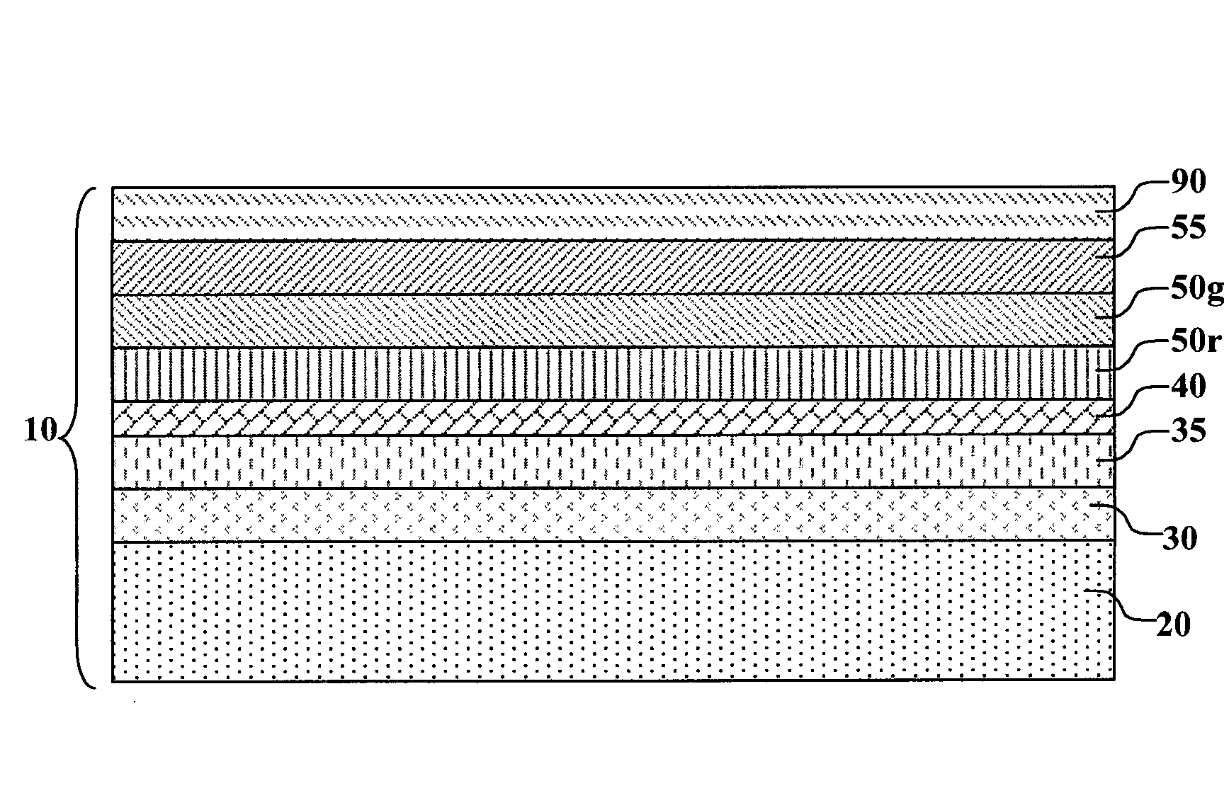
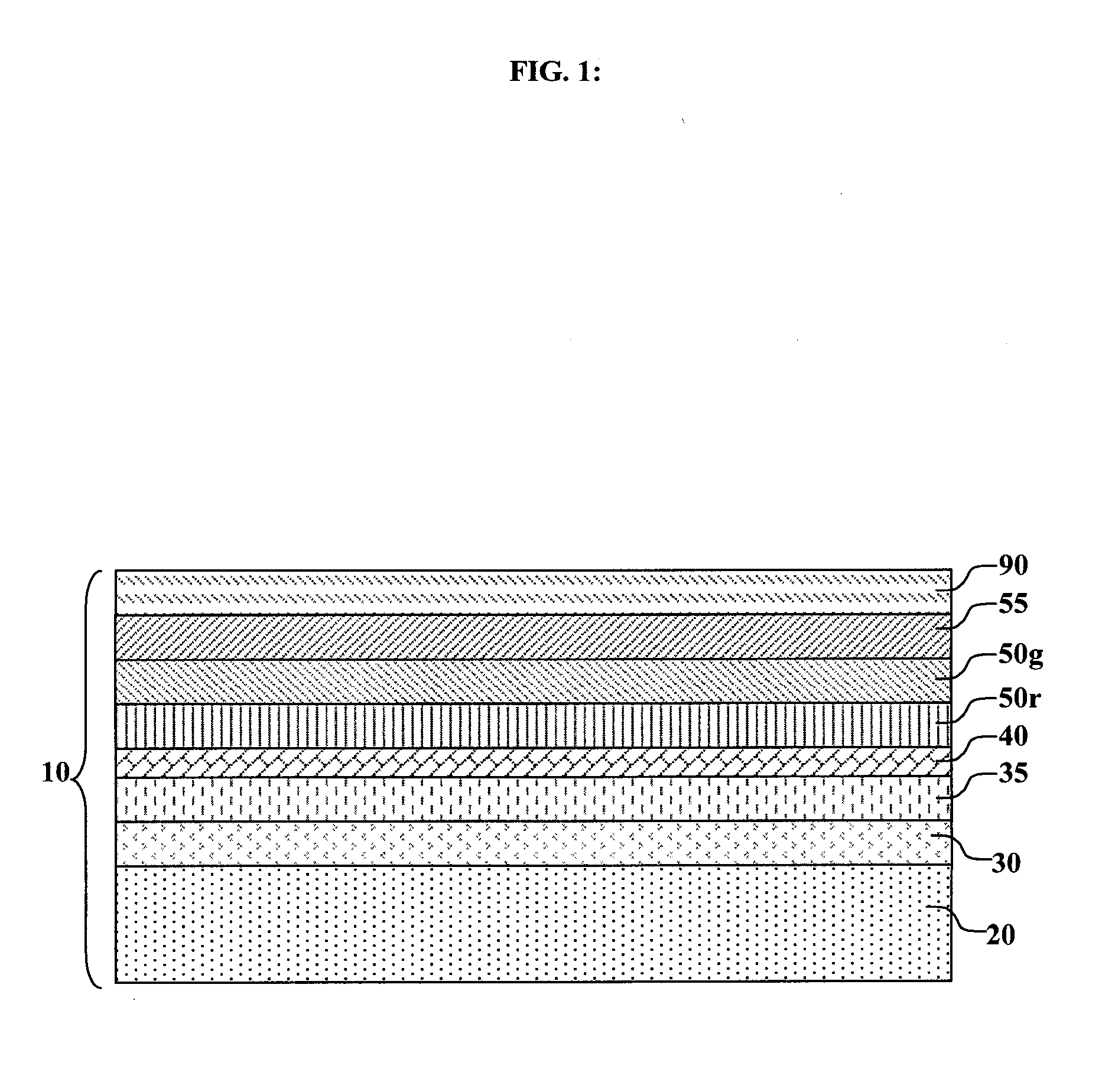
High-performance broadband OLED device
a broadband oled, high-performance technology, applied in the direction of layered products, chemistry apparatus and processes, and light-emitting compositions, can solve the problems of multi-layer broadband emitters and hue shift, and achieve the effect of improving efficiency and hue stability
- Summary
- Abstract
- Description
- Claims
- Application Information
AI Technical Summary
Benefits of technology
Problems solved by technology
Method used
Image

Examples
example 2 (
INVENTIVE)
[0093]An OLED device was constructed as described above for Example 1 except that Step 6 was as follows:[0094]6. The above-prepared substrate was further treated by vacuum-depositing a 40 nm green light-emitting layer including 90% PBNA as host and 10% 2,6-bis(diphenylamino)-9,10-diphenylanthracene as green emitting dopant.
example 3 (
INVENTIVE)
[0095]1. On top of a clean glass substrate, ITO was deposited by sputtering to form a transparent electrode of 60 nm thickness.[0096]2. The above-prepared ITO surface was treated with a plasma oxygen etch.[0097]3. The above-prepared substrate was further treated by vacuum-depositing a 10 nm layer of CHATP as an HIL.[0098]4. The above-prepared substrate was further treated by vacuum-depositing a 10 nm layer of NPB as an HTL.[0099]5. The above-prepared substrate was further treated by vacuum-depositing a 20 nm red light-emitting layer including 94.5% of NPB as a host and 5% PTBR as a yellow-emitting dopant with 0.5% TPDBP as a red emitting dopant.[0100]6. The above-prepared substrate was further treated by vacuum-depositing a 40 nm green light-emitting layer including 89% PBNA as a host, 10% 2,6-bis(diphenylamino)-9,10-diphenylanthracene as green emitting dopant, with 1% BEP as a stabilizer.[0101]7. A 40 nm mixed electron-transporting layer was vacuum-deposited, including 49...
example 4 (
INVENTIVE)
[0103]An OLED device was constructed as described above for Example 3 except that Step 6 was as follows:[0104]6. The above-prepared substrate was further treated by vacuum-depositing a 40 nm green light-emitting layer including 89.7% PBNA as a host, 10% 2,6-bis(diphenylamino)-9,10-diphenylanthracene as green emitting dopant, and 0.3% diphenylquinacridone (DPQ) as a stabilizer.
PUM
 Abstract
Description
Claims
Application Information