
Solar cell

a solar cell and cell technology, applied in the field of solar cells, can solve the problems of difficult to improve the efficiency of photon-electron conversion and difficult to reduce the cost of silicon-based materials

Inactive Publication Date: 2009-03-05
HON HAI PRECISION IND CO LTD
View PDF7 Cites 8 Cited by
  • Summary
  • Abstract
  • Description
  • Claims
  • Application Information

AI Technical Summary

Benefits of technology

[0007]What is needed, therefore, is a solar cell with fewer lattice defects and higher photon-electron conversion efficiency using the semi-conductive compounds.

Problems solved by technology

However, cost of the silicon based materials is hard to be reduced.
In addition, lattice defects, such as dislocations and stacking faults, are prone to occur in the semiconductor layers during formation when the semi-conductive compounds are used, and thus the efficiency of the photon-electron conversion is difficult to be improved.

Method used


Image

  • Solar cell
  • Solar cell

Examples


Embodiment Construction

[0012]Embodiments of the present solar cell will now be described in detail below and with reference to the drawing.

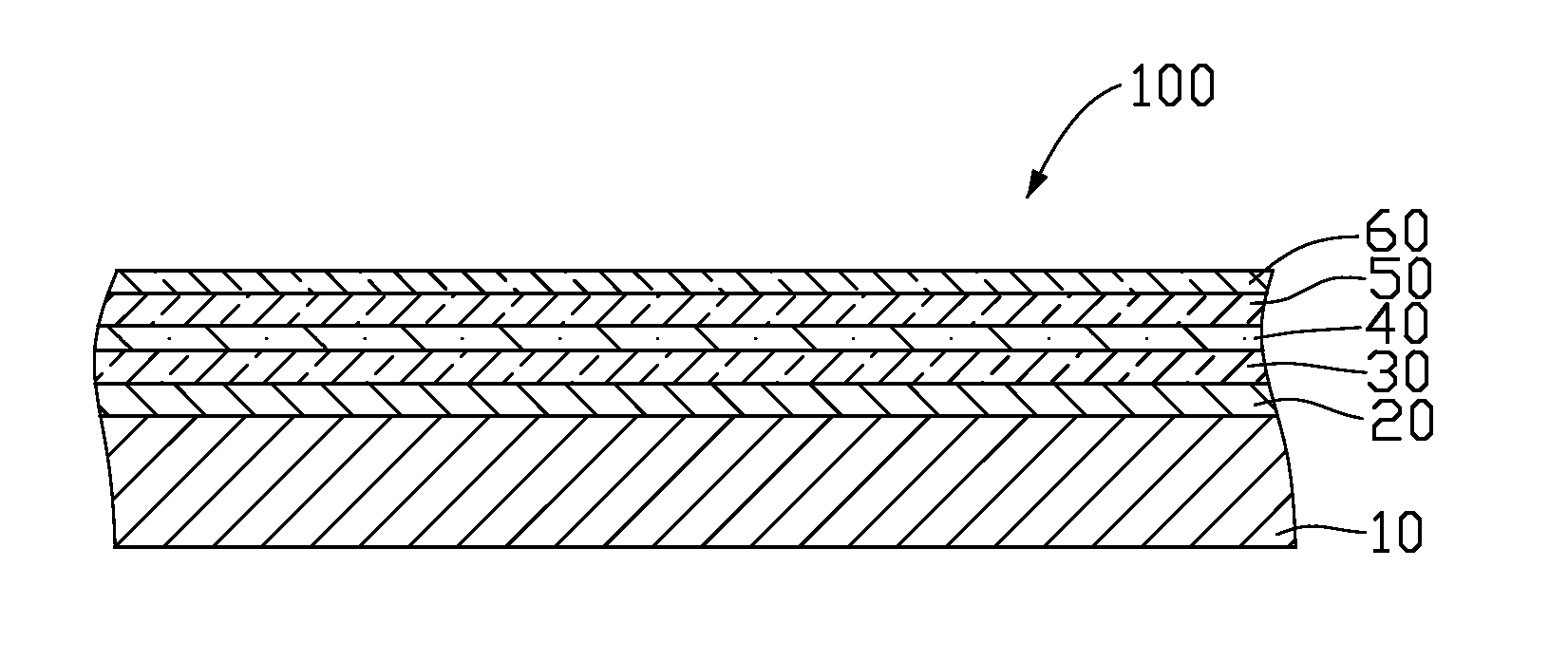
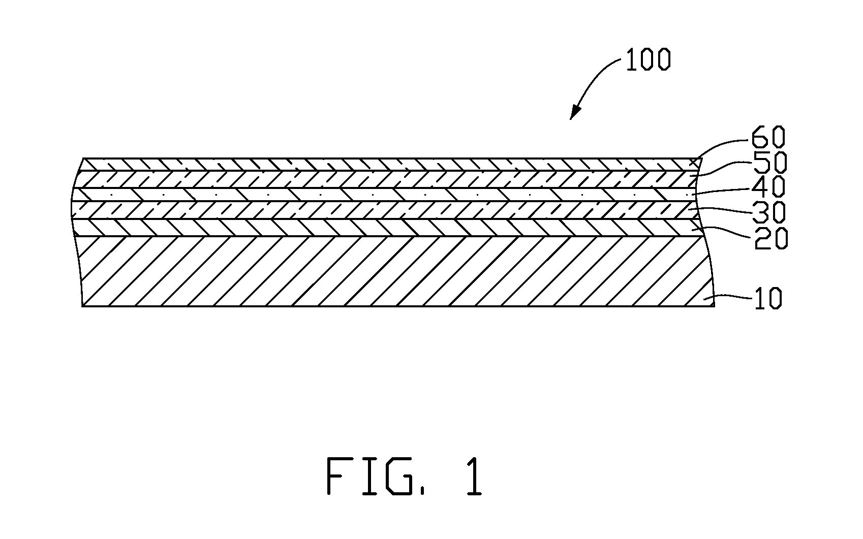
[0013]Referring to the drawing, an exemplary solar cell 100 is shown. The solar cell 100 includes a substrate 10, a back metal-contact layer 20, a P-type semiconductor layer 30, a P-N junction layer 40, an N-type semiconductor layer 50 and a transparent electrically conductive layer 60.

[0014]The substrate 10 can be rigid or flexible according to need. A material of the substrate 10 can be selected from glass, ceramic, plastic and stainless steel.

[0015]The back metal-contact layer 20 is comprised of a material selected from silver, copper, molybdenum, aluminum, copper aluminum alloy, silver copper alloy, and copper molybdenum alloy. The back metal-contact layer 20 is formed on the substrate 10 by DC magnetron sputtering.

[0016]The P-type semiconductor layer 30 is comprised of nano particles of a P-type semi-conductive compound. The P-type semi-conductive compound can be ...


PUM


Abstract

A solar cell includes a back metal-contact layer, a P-type semiconductor layer, a P-N junction layer, an N-type semiconductor layer and a transparent electrically conductive layer. The P-type semiconductor layer is formed on the back metal-contact layer. The P-type semiconductor layer is comprised of nano particles of a P-type semi-conductive compound. The P-N junction layer is formed on the P-type semiconductor layer. The N-type semiconductor layer is formed on the P-N junction layer. The N-type semiconductor layer is comprised of nano particles of an N-type semi-conductive compound. The transparent electrically conductive layer is formed on the N-type semiconductor layer and functions as a front contact layer.

Description

BACKGROUND[0001]1. Technical Field[0002]The present invention relates to solar cells, and particularly, to a solar cell made of semi-conductive compounds.[0003]2. Description of Related Art[0004]Currently, various solar cells have been designed to receive and convert sunlight into electrical energy. Such solar cells have been applied on roofs of buildings and cars, or applied on portable electronic devices.[0005]In a typical solar cell, a P-type semiconductor layer and an N-type semiconductor layer are two key components. When sunlight projects on surfaces of the P-type semiconductor layer or the N-type semiconductor layer, a part of the sunlight is unavoidably reflected by the surfaces, and the other is absorbed. Photons in the absorbed sunlight collide with electrons in the P-type semiconductor layer or the N-type semiconductor layer, thereby, electron-hole pairs are generated, and thus an electric field is formed between the P-type semiconductor layer and the N-type semiconductor...

Claims


Application Information

Patent Timeline
Patent Type & Authority Applications(United States)
IPC IPC(8): H01L31/0264H01L31/04
CPCH01L31/035272H01L31/022466
Inventor CHEN, GA-LANE
Owner HON HAI PRECISION IND CO LTD
Learn More