Wafer level phosphor coating technique for warm light emitting diodes

a light-emitting diode and phosphor coating technology, applied in the direction of semiconductor devices, semiconductor/solid-state device details, electrical devices, etc., can solve the problems of non-uniform color temperature led, difficult to control and the difficulty of stenciling the geometry and thickness of the phosphor layer

Active Publication Date: 2009-03-05
CREELED INC
View PDF95 Cites 143 Cited by
  • Summary
  • Abstract
  • Description
  • Claims
  • Application Information

AI Technical Summary

Problems solved by technology

Using this method, however, it can be difficult to control the phosphor layer's geometry and thickness.
As a result, light emitting from the LED at different angles can pass through different amounts of conversion material, which can result in an LED with non-uniform color temperature as a function of viewing angle.
Like the syringe method above, using the stencil method can be difficult to control the geometry and layer thickness of the phosphor containing polymer.
The stenciling composition may not fully fill the stencil opening such that the resulting layer is not uniform.
These problems can result in LEDs having non-uniform color temperature and LEDs that are difficult to consistently reproduce with the same or similar emission characteristics.
With these approaches one challenge is accessing the wire bond pad on the device after the coating process.
Accessing the wire bond by standard wafer fabrication techniques is difficult with typical silicone binding material, as well as other binder materials such as epoxies or glass.
Silicones are not compatible with commonly used wafer fabrication materials such as acetone, as well as some developers and resist strippers.
This can limit the options and choices of process steps for the particular silicones.
Cured silicone films with phosphor are also difficult to etch and have a very slow etch rate in chlorine and CF4 plasma, and wet etching of cured silicones is typically inefficient.
Perceptible variations in color emitted by packages designed to emit a single color of light can reduce customer satisfaction and reduce overall acceptance of LED packages for commercial uses.
Each phosphor absorption and re-emission results in Stokes losses and the overlap of the spectrum as shown in FIG. 3 can reduce the overall emission efficiency by greater than 30%.
As one example, certain yellow phosphors such as YAG can be more sensitive to heat compared to red phosphors and the efficacy of these YAG phosphors can degrade over time.

Method used


Image

  • Wafer level phosphor coating technique for warm light emitting diodes
  • Wafer level phosphor coating technique for warm light emitting diodes
  • Wafer level phosphor coating technique for warm light emitting diodes

Examples


Embodiment Construction

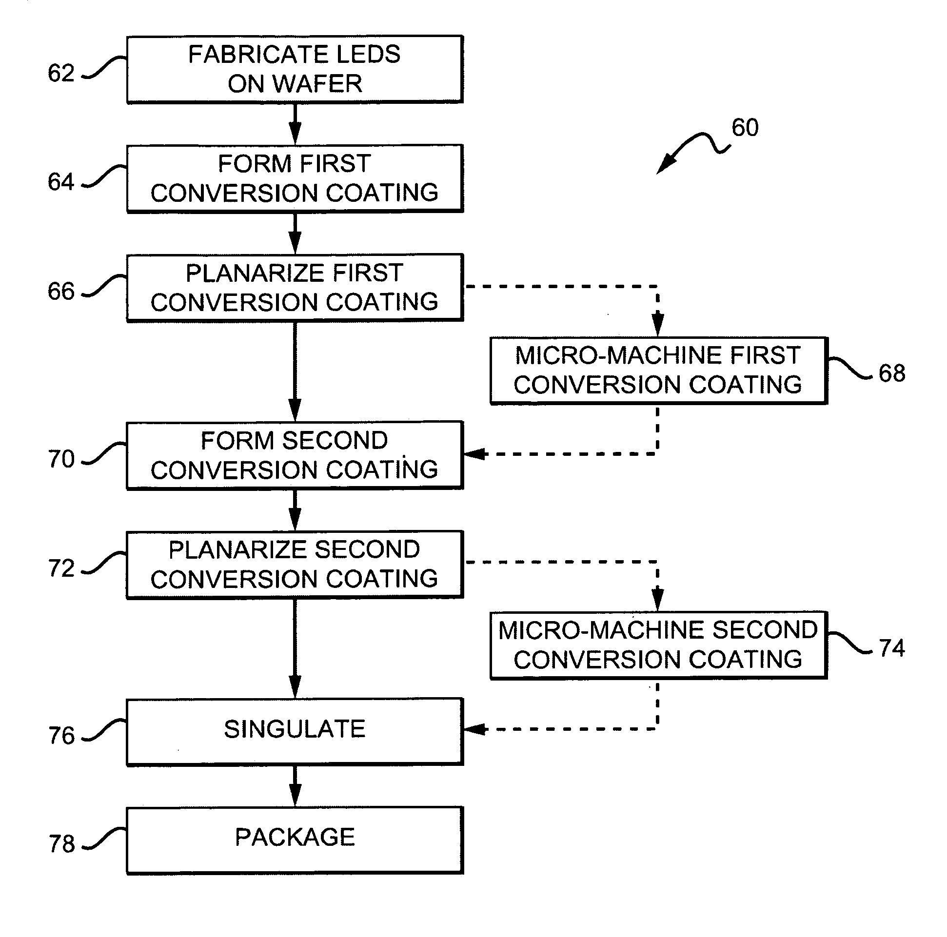
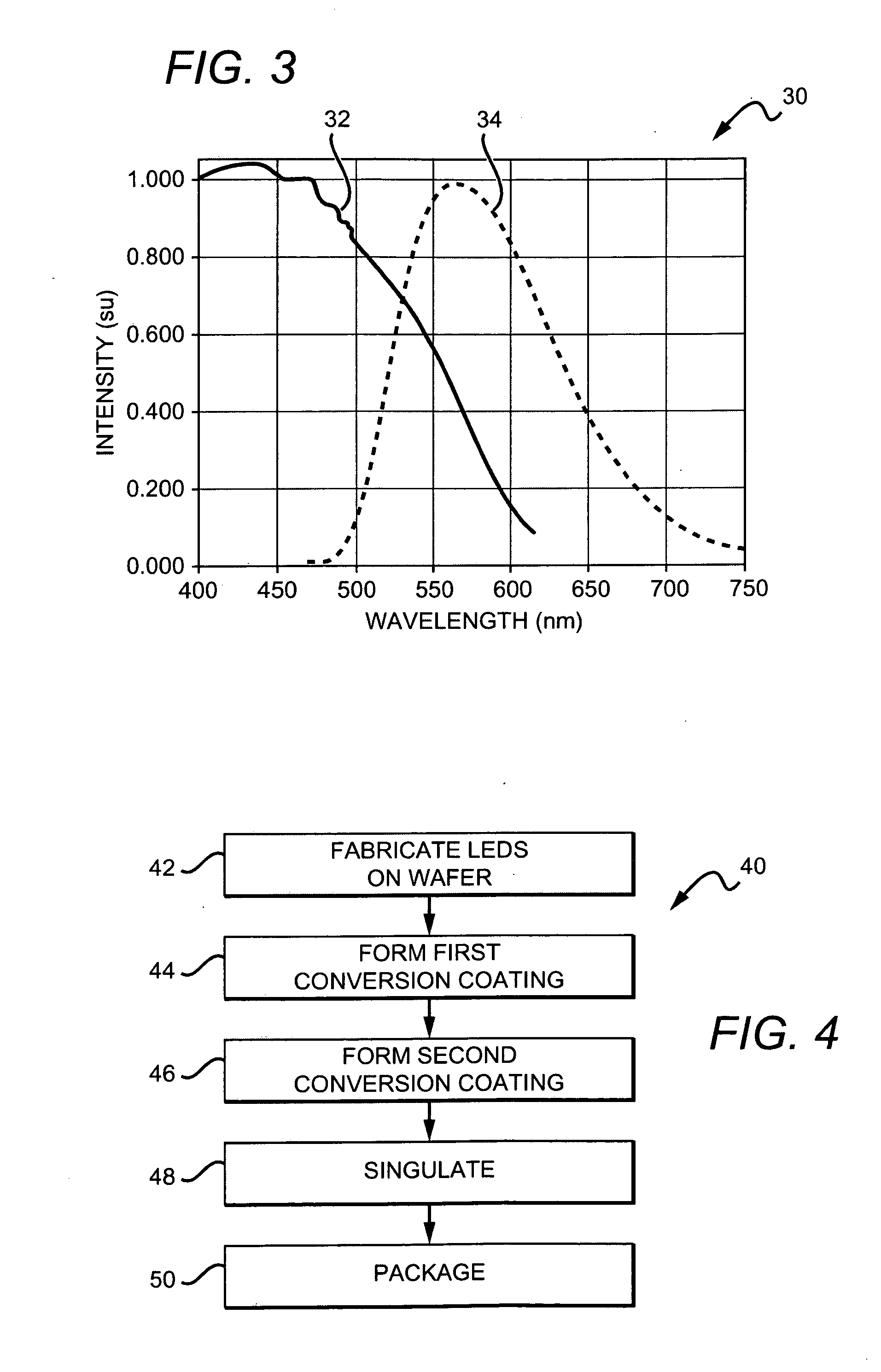
[0045]The present invention discloses new methods for fabricating semiconductor devices such as LED chips, with one embodiment of a fabrication method according to the present invention providing LED chip fabrication at the wafer level. The present invention also discloses LED chips and LED packages fabricated using the methods. Different embodiments of the present invention disclose sequential coating methods that provide two or more coatings or layers of conversion material over LEDs. In one embodiment this can be done at the wafer level. The methods according to the present invention are particularly applicable to fabricating LED chips that emit a warm white light, which typically requires covering LEDs with two or more phosphors such as yellow and red phosphors. As described above, the presence of the two phosphors in the same layer can result in re-absorption losses due to a portion of the emission spectra from one of the phosphors overlapping with the excitation spectrum of on...


PUM


Abstract

Methods for wafer level fabricating of light emitting diode (LED) chips are disclosed with one embodiment of a method according to the present invention comprising providing a plurality of LEDs and then coating of the LEDs with a layer of first conversion material so that at least some light from the LEDs passes through the first conversion material. The light is converted to different wavelengths of light having a first conversion material emission spectrum. The LEDs are then coated with a layer of second conversion material arranged on the first layer of conversion. The second conversion material has a wavelength excitation spectrum, and at least some light from the LEDs passes through the second conversion material and is converted. The first conversion material emission spectrum does not substantially overlap with the second conversion material excitation spectrum. Methods according to the present invention can also be used in wafer level fabrication of LED chips and LED packages with pedestals for electrically contacting the LEDs through the conversion coatings.

Description

[0001]This application is a continuation-in-part of and claims the benefit of U.S. Patent Application Publication Numbers 2008 / 0173884 filed on Jan. 22, 2007, and 2008 / 0179611 filed on Sep. 7, 2007, both to Chitnis et al.BACKGROUND OF THE INVENTION[0002]1. Field of the Invention[0003]This invention relates to methods for fabricating solid state emitters and in particular methods for tuning the emission characteristics of light emitting diodes coated by a conversion material.[0004]2. Description of the Related Art[0005]Light emitting diodes (LED or LEDs) are solid state devices that convert electric energy to light, and generally comprise one or more active layers of semiconductor material sandwiched between oppositely doped layers. When a bias is applied across the doped layers, holes and electrons are injected into the active layer where they recombine to generate light. Light is emitted from the active layer and from all surfaces of the LED.[0006]Conventional LEDs cannot generate ...

Claims


Application Information

Patent Timeline
Patent Type & Authority Applications(United States)
IPC IPC(8): H01L33/00H01L21/00H01L33/38H01L33/44H01L33/50H01L33/62
CPCH01L23/3114H01L33/38H01L33/44H01L2224/16H01L33/62H01L2933/0041H01L33/504
Inventor CHAKRABORTY, ARPAN
Owner CREELED INC
Why Eureka
Try Eureka