

Semiconductor device
a technology of semiconductor devices and semiconductors, applied in semiconductor devices, semiconductor/solid-state device details, electrical apparatus, etc., can solve the problems of increasing the complexity of wiring on the wafers, increasing the difficulty of electrical connection, and increasing the proportion of electrodes that are not connected, so as to achieve high-reliability electrical connection
- Summary
- Abstract
- Description
- Claims
- Application Information
AI Technical Summary
Benefits of technology
Problems solved by technology
Method used
Image

Examples
first embodiment
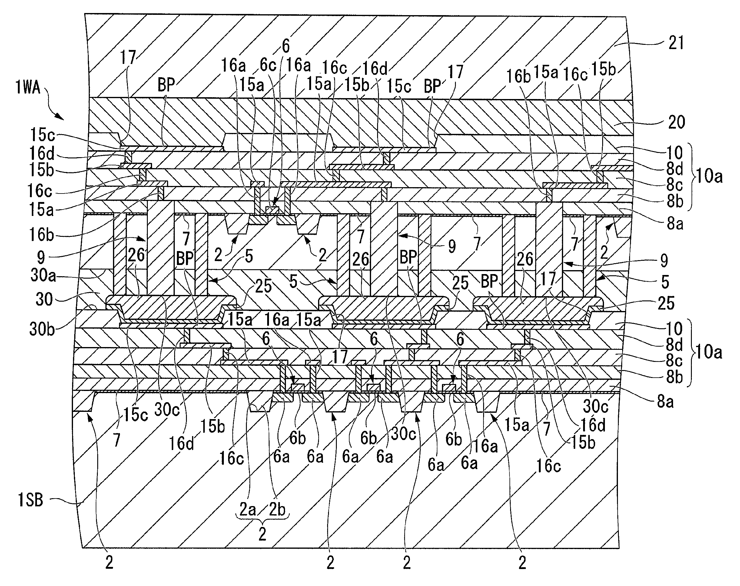
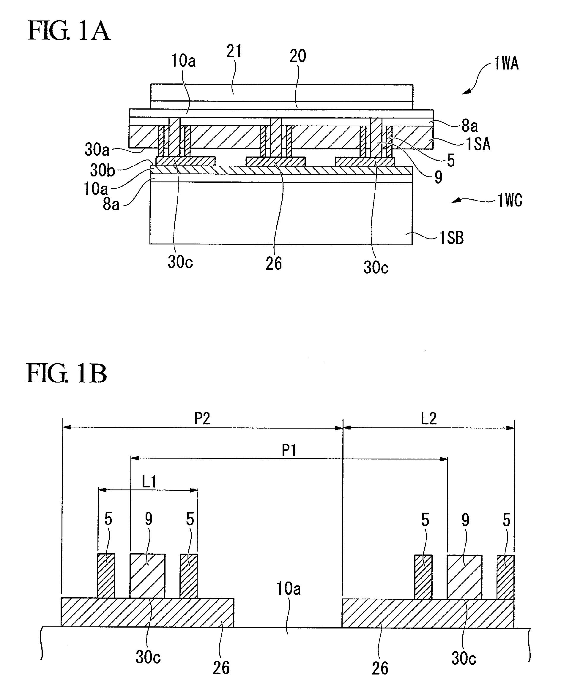
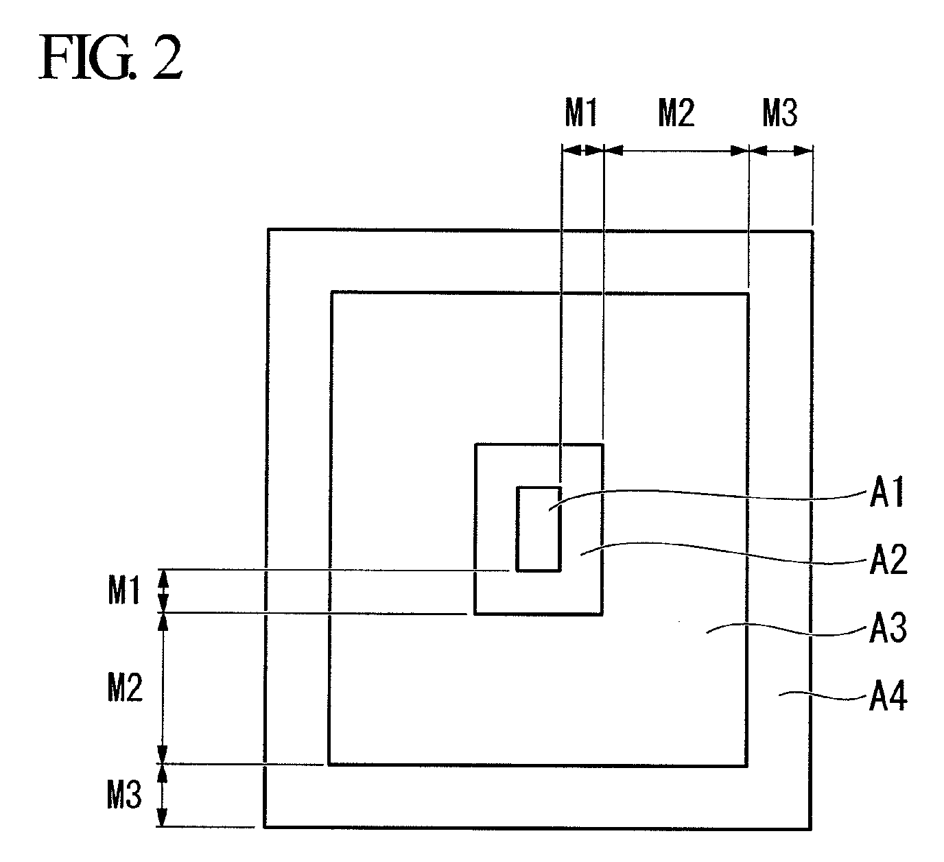
[0069]FIGS. 1A to 20 are explanatory views of a first embodiment of the semiconductor device of the invention. FIG. 19 is a cross-sectional view of primary parts of the semiconductor device of this embodiment. FIGS. 1A and 1B are enlarged cross-sectional schematic views of a part of the semiconductor device of this embodiment. FIG. 2 is an explanatory plan view of the relationship between the size of a penetrating wiring part and a bump in the semiconductor device of this embodiment. FIGS. 3 to 18 are explanatory views of manufacturing processes of the semiconductor device of this embodiment. FIG. 20 is an explanatory flowchart of a manufacturing process of the semiconductor device of this embodiment.
[0070]In the semiconductor device of the embodiment shown in FIG. 19, an upper wafer 1WA and a lower wafer 1WB are bonded together. The wafer 1WA and the wafer 1WB are manufactured by processing substrates 1SA and 1SB. A bonding surface 30a of the upper wafer 1WA is arranged opposite th...
second embodiment
[0139]FIGS. 22 to 42 are explanatory views of a semiconductor device according to a second embodiment. FIG. 41 is a cross-sectional view of primary parts of an example of the semiconductor device of the invention, FIG. 22 is an enlarged schematic view of one part of the semiconductor device shown in FIG. 41, and FIG. 23 is an explanatory plan view of the relationship between the size of a penetrating wiring part and a bump in the semiconductor device shown in FIG. 22. FIGS. 24 to 40 are explanatory views of processes of manufacturing the semiconductor device shown in FIG. 41, and FIG. 42 is an explanatory flowchart of processes of manufacturing the semiconductor device shown in FIG. 41.
[0140]In the semiconductor device of the embodiment shown in FIGS. 22 to 42, like members to those in FIG. 18 are designated with like reference numerals, and are not repetitiously explained.
[0141]The semiconductor device of the embodiment shown in FIG. 41 differs from the semiconductor device shown i...
experimental example
[0191]Using a silicon substrate having a diameter of 200 mm (eight inches) and a thickness of 30 μm, an upper wafer having penetrating isolation parts and penetrating wiring parts formed thereon was made in the same manner as the upper wafer 1WA of the semiconductor device shown in FIG. 19.
[0192]The penetrating wiring part on the upper wafer 1WA includes two wiring parts made of tungsten, whose cross-sectional shape is that of a rectangle having a vertical dimension of 5.6 μm and a horizontal dimension of 1.5 μm, these being arranged in parallel with an interval of 2.6 μm between them. The length of the penetrating protrusions in the thickness direction of the wafer 1WA was 40 μm. In the design of the pre-processed substrate, the pitch for arranging the penetrating wiring parts was set at 50 μm. The penetrating isolation parts are square frames having external length and width of 13.4 μm.
[0193]For the upper wafer 1WA thus obtained, a positioning margin was determined (i.e. the diffe...
PUM
 Abstract
Description
Claims
Application Information