Light emitting display device and method for fabricating the same

a technology of light emitting display and manufacturing method, which is applied in the direction of discharge tube luminescnet screen, discharge tube/lamp details, electric discharge lamps, etc., can solve the problems of increasing fabrication cost and processing time, and achieve the effect of reducing the thickness of the light emitting display devi

Active Publication Date: 2009-03-05
SAMSUNG DISPLAY CO LTD
View PDF8 Cites 35 Cited by
  • Summary
  • Abstract
  • Description
  • Claims
  • Application Information

AI Technical Summary

Benefits of technology

[0008]The present embodiments solve drawbacks of the prior art, and therefore an object of the present embodiments is to provide a light emitting display device including a second substrate which is not formed with grooves in order to reduce the thickness of the light emitting display device, and a method for fabricating the same.

Problems solved by technology

To form the cavity-shaped second substrate, grooves are formed on a flat glass using an etching solution (HF), which causes increases in fabrication cost and processing time.

Method used


Image

  • Light emitting display device and method for fabricating the same
  • Light emitting display device and method for fabricating the same
  • Light emitting display device and method for fabricating the same

Examples


Embodiment Construction

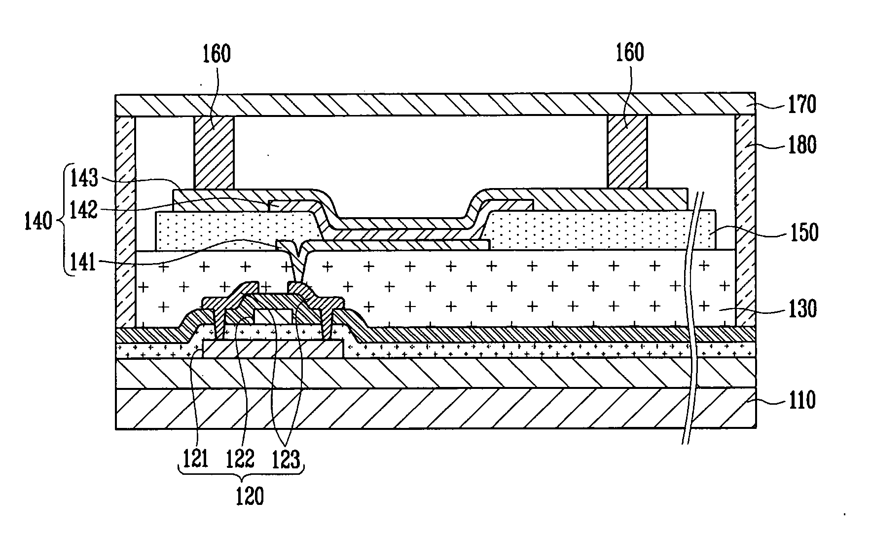
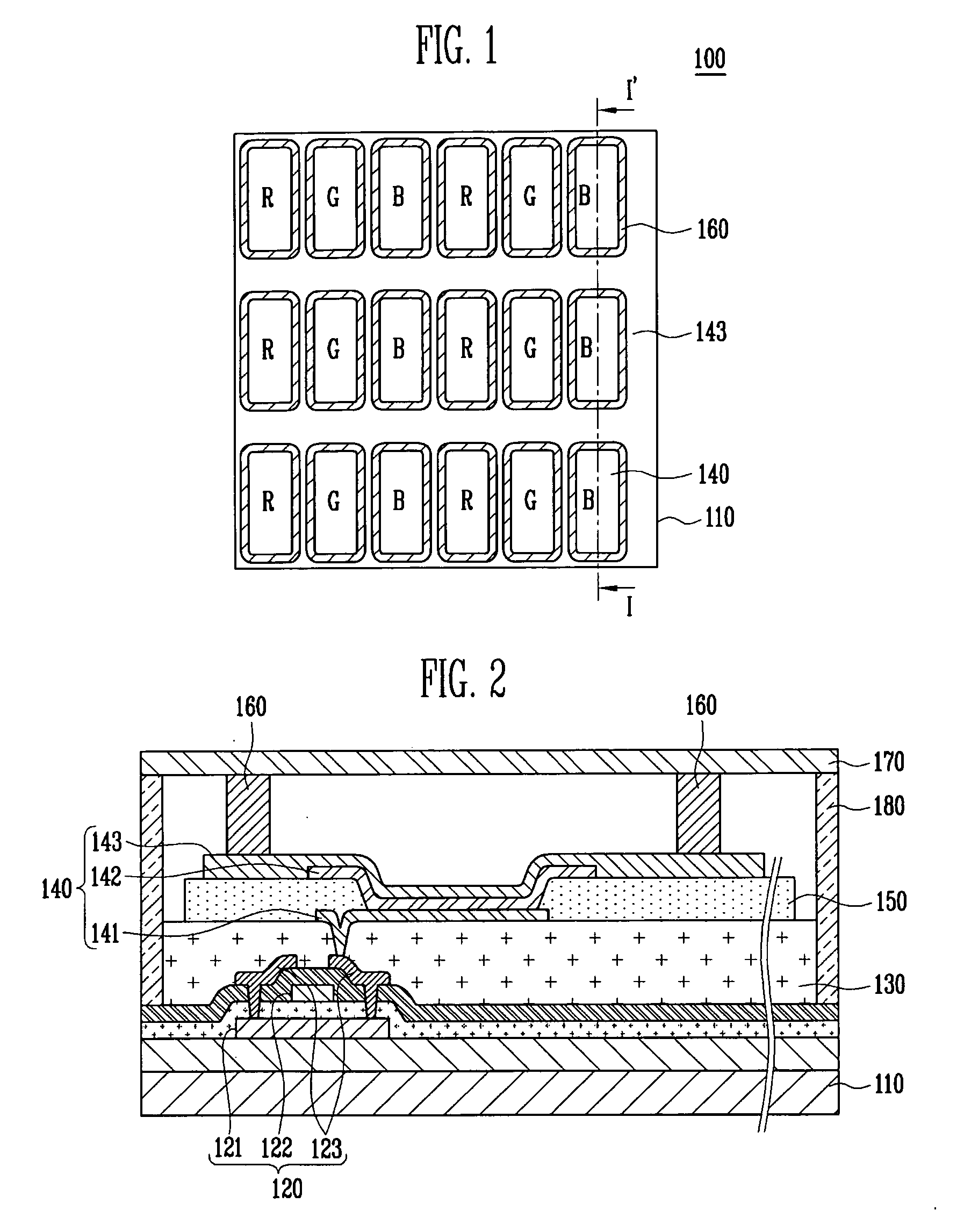
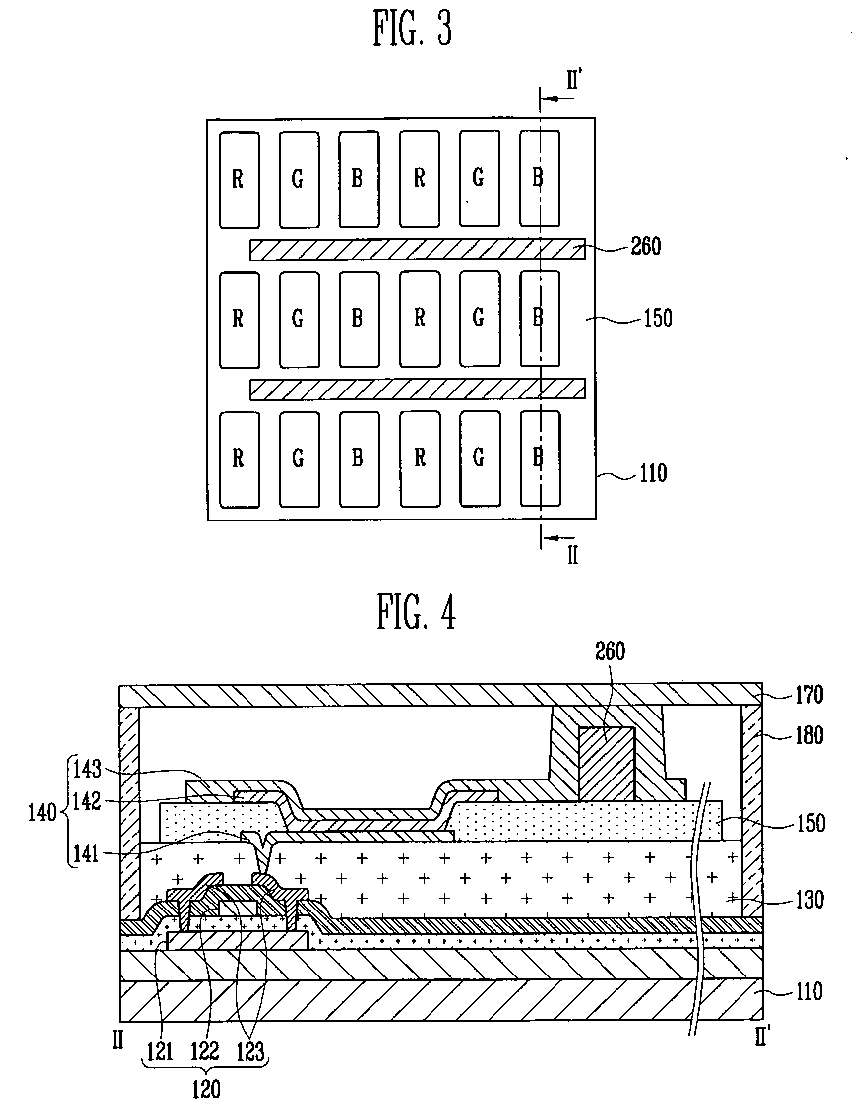
[0021]In the following detailed description, only certain exemplary embodiments have been shown and described, simply by way of illustration. As those skilled in the art would realize, the described embodiments may be modified in various different ways, all without departing from the spirit or scope of the present embodiments. Accordingly, the drawings and description are to be regarded as illustrative in nature and not restrictive. In addition, when an element is referred to as being “on” another element, it can be directly on the element or be indirectly on the element with one or more intervening elements interposed therebetween. Also, when an element is referred to as being “connected to” another element, it can be directly connected to the element or be indirectly connected to the element with one or more intervening elements interposed therebetween. Hereinafter, like reference numerals refer to like elements.

[0022]FIG. 1 is a plan view schematically showing a pixel array of an...


PUM


Abstract

Disclosed are a light emitting display device and a method for fabricating the same. The light emitting display device according to the present embodiments includes a first substrate including a pixel region and a non-pixel region surrounding the pixel region; a plurality of light emitting diodes disposed in the pixel region of the first substrate, and each including a first electrode, a light emitting layer, and a second electrode; and a second substrate disposed to face the first substrate. Also, the light emitting display device according to the present embodiments includes a sealant by coupling the first substrate to the second substrate to encapsulate the pixel region; and a spacer disposed between the first substrate and the second substrate and provided in a non-light emission region arranged between the adjacent light emitting diodes. In this case, the spacer is disposed on the second electrode of the non-light emission region to be in contact with the second substrate.

Description

CROSS-REFERENCE TO RELATED APPLICATION[0001]This application claims priority to and the benefit of Korean Patent Application No. 10-2007-0089934 filed on Sep. 5, 2007 in the Korean Intellectual Property Office, the entire content of which is incorporated herein by reference.BACKGROUND OF THE INVENTION[0002]1. Field of the Invention[0003]The present embodiments relate to a light emitting display device capable of decreasing in thickness, and a method for fabricating the same.[0004]2. Description of the Related Art[0005]An organic light emitting display device emits light by electrically exciting a fluorescent organic compound. Such organic light emitting display device is attracting attention as a next-generation of display device since it is driven at a low voltage and easily manufactured in small and slim scales, and also has a wide viewing angle, short response time, etc.[0006]An organic light emitting display device includes a first substrate; at least one organic light emitting ...

Claims


Application Information

Patent Timeline
Patent Type & Authority Applications(United States)
IPC IPC(8): H01J1/62
CPCH01L51/5237H05B33/10H05B33/04H10K50/8428H10K50/8426H10K50/84
Inventor JOO, YOUNG-CHEOLLEE, KWAN-HEESONG, SEUNG-YONGSON, JONG-HOONCHOI, YOUNG-SEO
Owner SAMSUNG DISPLAY CO LTD
Why Eureka
Try Eureka