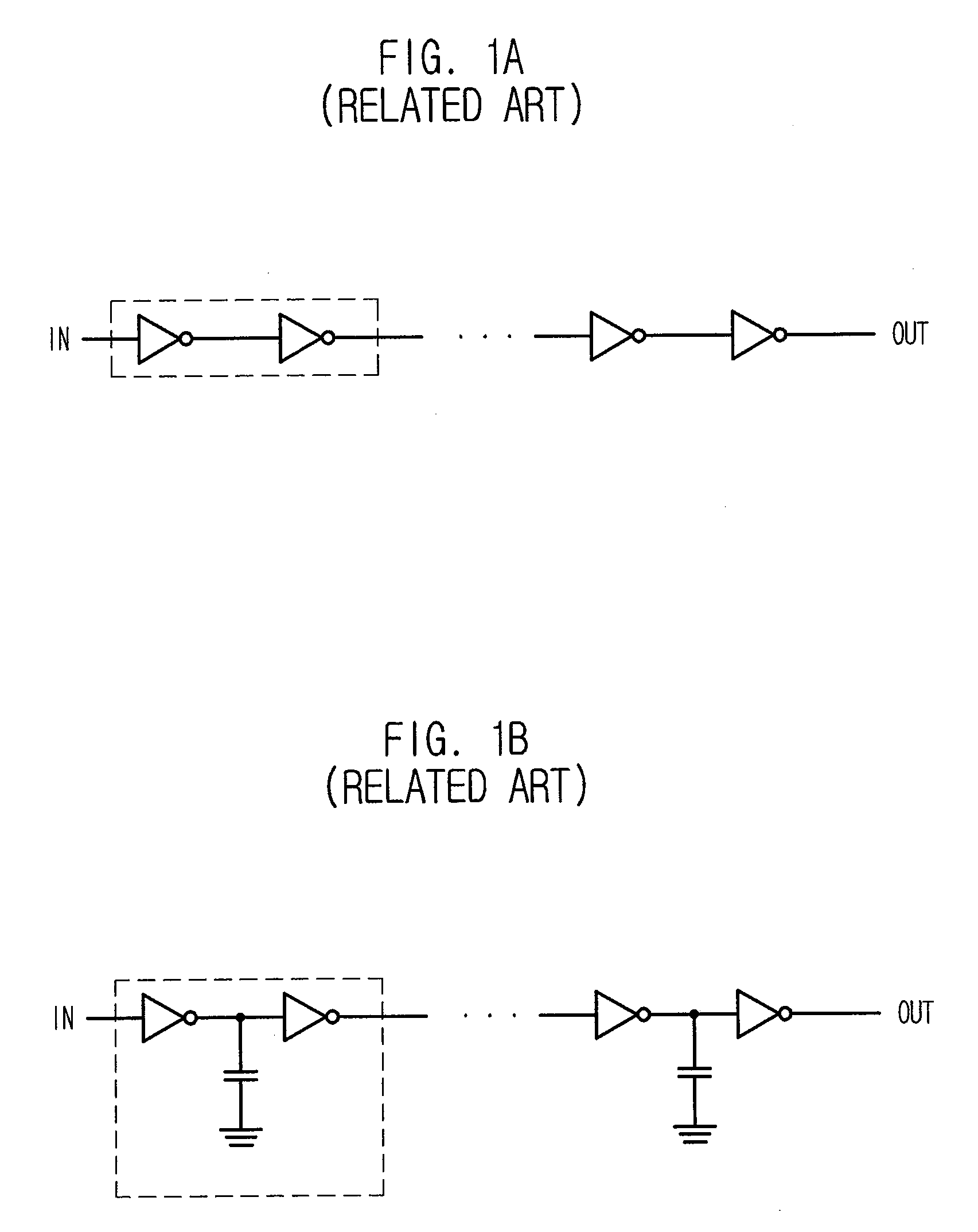
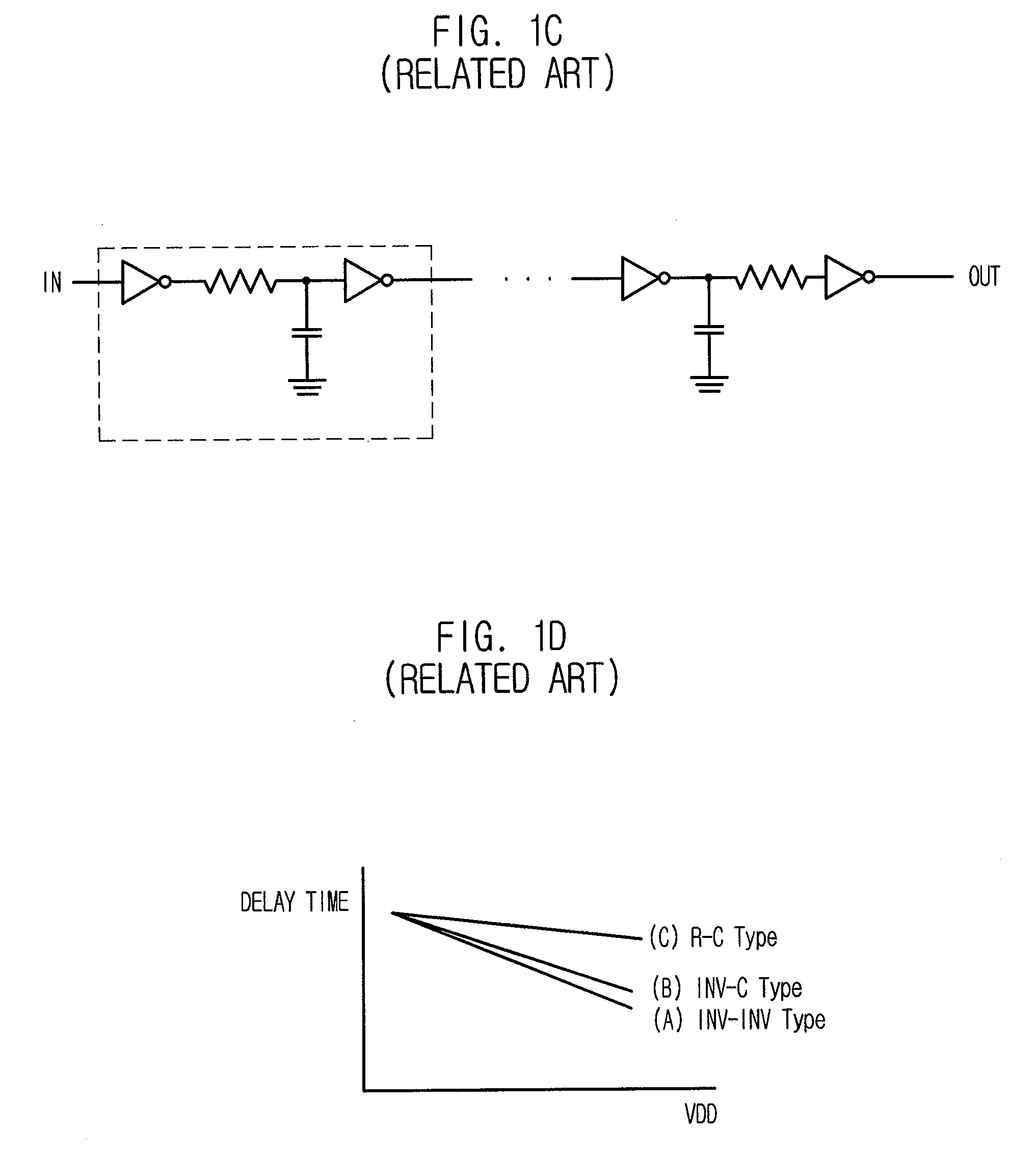
Delay circuit

a delay circuit and delay time technology, applied in the field of semiconductor devices, can solve the problems of not being able to independently control or adjust the delay time according, and achieve the effect of rapidly changing the load capacitance or resistance, and easily controlling the delay time dependen

Inactive Publication Date: 2009-03-05
SK HYNIX INC
View PDF6 Cites 3 Cited by
  • Summary
  • Abstract
  • Description
  • Claims
  • Application Information

AI Technical Summary

Benefits of technology

[0013]It is, therefore, an object of the present invention to provide a delay circuit that can control delay time at a high operating voltage and a low operating voltage independently and easily.
[0017]The delay circuit in accordance with the present invention can easily control the dependence of the delay time on the power supply voltage by rapidly varying the load capacitance or resistance according to the change of the power supply voltage.

Problems solved by technology

Although the conventional delay circuits of FIGS. 1A to 1C have different variation ranges with respect to the change of the power supply voltage, they cannot independently control or adjust the delay time according to the change of the power supply voltage because the delay time changes linearly.

Method used


Image

  • Delay circuit
  • Delay circuit
  • Delay circuit

Examples


first embodiment

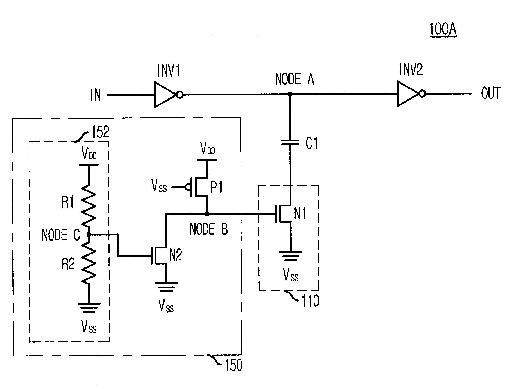
[0036]FIG. 2A is a circuit diagram of a delay circuit in accordance with the present invention.

[0037]The delay circuit 100A includes first and second inverters INV1 and INV2, a capacitor C1, a switching unit 110, and a power supply voltage detector 150. The capacitor C1 has one terminal connected to a node A of a delay line IN-OUT, and the switching unit 110 is connected between the other terminal of the capacitor C1 and a ground terminal VSS. The power supply voltage detector 150 detects whether a power supply voltage VDD is higher or lower than a predetermined threshold voltage, and controls on / off operation of the switching unit 110. The threshold voltage is a preset voltage and can be changed by a designer.

[0038]The power supply voltage detector 150 turns off the switching unit 110 when the power supply voltage VDD is higher than the threshold voltage, and turns on the switching unit 110 when the power supply voltage VDD is lower than the threshold voltage.

[0039]The switching un...

second embodiment

[0048]FIG. 3A is a circuit diagram of a delay circuit in accordance with the present invention. The delay circuit 100B includes first and second inverters INV3 and INV4, a capacitor C2, a switching unit 120, and a power supply voltage detector 160. The delay circuit 100B further includes a third inverter INV5 in comparison with the delay circuit 100A.

[0049]The third inverter INV5 is connected between the power supply voltage detector 160 and the switching unit 120. Unlike the delay circuit of FIG. 2A, the delay circuit of FIG. 3A turns off the switching unit 120 when the power supply voltage VDD is lower than the threshold voltage, and turns on the switching unit 120 when the power supply voltage VDD is higher than the threshold voltage.

[0050]Consequently, the capacitor does not act as the load in the delay line IN-OUT when the power supply voltage VDD is lower than the threshold voltage. On the other hand, the capacitor acts as the load in the delay line IN-OUT when the power suppl...

third embodiment

[0056]FIG. 4A is a circuit diagram of a delay circuit in accordance with the present invention.

[0057]The delay circuit 200A includes first and second inverters INV6 and INV7, a capacitor C3, a first resistor R3, a switching unit 210, and a power supply voltage detector 250. The first resistor R3 is connected between an output terminal of the first inverter INV6 and an input terminal of the second inverter INV7. The first inverter INV6 and the second inverter INV7 constitute a delay line IN-OUT. The switching unit 210 is connected in parallel to the first resistor R3 between the output terminal of the first inverter INV6 and the input terminal of the second inverter INV7. The power supply voltage detector 250 detects whether a power supply voltage VDD is higher or lower than a desired threshold voltage, and controls on / off operation of the switching unit 210.

[0058]The power supply voltage unit 250 turns on the switching unit 210 when the power supply voltage VDD is higher than the th...


PUM


Abstract

A delay circuit controls a delay time according to variation of a power supply voltage. In the delay circuit, the capacitance of a capacitor connected in parallel to the delay line is changed according to the change of the power supply voltage. Alternatively, a current is made to flow through one path selected from a plurality of paths having different resistance between the input and the output of the delay line. Accordingly, the delay time can be independently controlled or adjusted by greatly changing the time taken to pass through the delay line according to the change of the power supply voltage.

Description

FIELD OF THE INVENTION[0001]The present invention relates to a semiconductor device, and more particularly, to a delay circuit for controlling a delay time according to variation of a power supply voltage.DESCRIPTION OF RELATED ART[0002]A delay circuit is a basic circuit that is widely used to determine order of internal control signals in Dynamic Random Access Memory (DRAM) and Application-Specific Integrated Circuit (ASIC).[0003]FIG. 1A is a circuit diagram illustrating an example of a conventional delay circuit.[0004]The delay circuit of FIG. 1A is an inverter chain type delay circuit with a plurality of inverters and determines a delay signal only using logic delay time.[0005]FIG. 1B is a circuit diagram illustrating another example of a conventional delay circuit.[0006]The delay circuit of FIG. 1B is a capacitor-type delay circuit that determines a delay signal by using time taken to charge and discharge a capacitor through logic gates.[0007]FIG. 1C is a circuit diagram illustr...

Claims


Application Information

Patent Timeline
Patent Type & Authority Applications(United States)
IPC IPC(8): H03H11/26
CPCH03H11/265G11C5/143G11C5/147G11C7/22G11C11/4074G11C11/4076G11C2207/2272
Inventor RHO, KWANG-MYOUNG
Owner SK HYNIX INC
Why Eureka
Try Eureka