

Semiconductor device having multiport memory
a technology of semiconductor devices and memory, applied in semiconductor devices, digital storage, instruments, etc., can solve the problems of difficult to sufficiently predict the degree of mutual interference, possible delay in the rise time (or fall time) of waveforms, and similar problems accompanying asynchronous operations. , to achieve the effect of reducing interference, expanding noise margin, and increasing circuit area
- Summary
- Abstract
- Description
- Claims
- Application Information
AI Technical Summary
Benefits of technology
Problems solved by technology
Method used
Image

Examples
embodiment 1
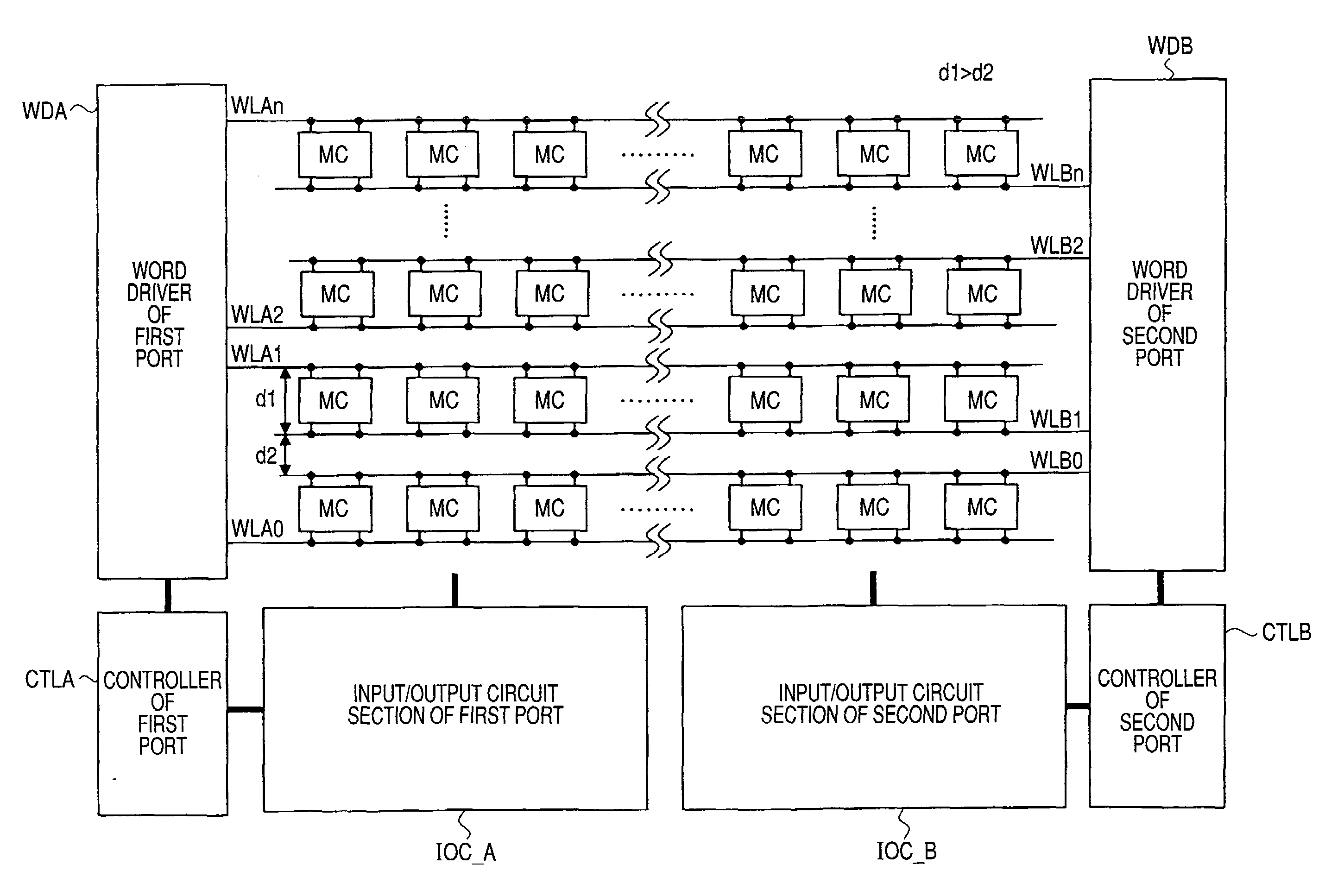
[0044][Embodiment 1]FIG. 1 shows a block diagram illustrating one exemplary configuration of a semiconductor device according to an embodiment 1 of the present invention. FIG. 2 shows a circuit diagram illustrating an exemplary configuration of a memory cell MC in the semiconductor device shown in FIG. 1. The semiconductor device shown in FIG. 1 includes a plurality of memory cells MC disposed in the row and column shape (matrix shape), a word driver WDA for a first port (port A), a controller CTLA and an input / output circuit section IOC_A, and further, a word driver WDB for a second port (port B), a controller CTLB and an input / output circuit section IOC_B.
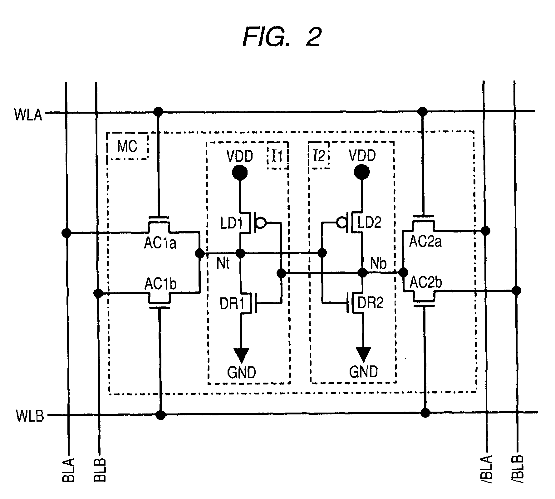
[0045]As shown in FIG. 2, each memory cell MC is a so-called SRAM memory cell, which includes two driver transistors DR1 and DR2, two load transistors LD1 and LD2, and four access transistors AC1a, AC1b, AC2a and AC2b. Here, the driver transistors DR1, DR2 and access transistors AC1a, AC1b, AC2a, AC2b are configured of NMOS trans...
embodiment 2
[0076][Embodiment 2]FIG. 7 shows a plan view illustrating an exemplary configuration of a semiconductor device deformed from the layout shown in FIG. 4, according to the present invention. As shown in FIG. 7, the semiconductor device according to the present embodiment 2 has a principal feature of further providing a shield line SLD, which extends in juxtaposition with the word line between the word lines of different ports (between WLA and WLB), in addition to the word line layout similar to FIG. 4.
[0077]With the provision of such the shield line SLD, it becomes possible to further expand a noise margin between the word lines of different ports. Also, if the layout area of each memory cell can be restrained, it becomes possible to further decrease the pitch d1 between WLA and WLB as compared with the pitch d1 in case of FIG. 4 due to a shield effect, and thus, it becomes possible to expand the noise margin with a smaller area than the case of embodiment 1.
[0078]Also, since the orde...
embodiment 3
[0087][Embodiment 3]FIG. 14 shows a block diagram illustrating one exemplary configuration of a semiconductor device according to the present invention. As compared with the semiconductor device shown in FIG. 1, the principal features of the semiconductor device shown in FIG. 14 lie in: (1) the disposition of input / output circuit sections IOC_A, IOC_B; (2) the wiring layout from the bit line to the IOC_A, IOC_B; and (3) the disposition of each control line when the controllers CTLA, CTLB control the IOC_A, IOC_B. In the following, descriptions on the portions overlapped with FIG. 1 are omitted.
[0088]In FIG. 14, the controller CTLA of a first port (port A) includes a latch section ADD_LT for latching an address signal for the first port being input externally, a decoder DEC for decoding the above address signal, and a Y selection buffer section YSEL_BF for outputting a Y selection signal etc. corresponding to a Y address for the first port. Similarly, the controller CTLB of a second ...
PUM
 Abstract
Description
Claims
Application Information