Method for metallizing a pattern in a dielectric film

a dielectric film and pattern technology, applied in the direction of basic electric elements, electrical equipment, semiconductor/solid-state device manufacturing, etc., can solve the problems of metal hard masks, dielectric material damage,

Inactive Publication Date: 2009-03-05
TOKYO ELECTRON LTD
View PDF12 Cites 20 Cited by
  • Summary
  • Abstract
  • Description
  • Claims
  • Application Information

AI Technical Summary

Benefits of technology

[0010]Additionally, the invention relates to a method for metallizing a pattern in a dielectric film. For example, the dielectric film can inc...

Problems solved by technology

However, with the implementation of low dielectric constant (low-k) and ultra-low-k dielectric materials in BEOL structures, it has been recognized that the processes utilized for removing the lithographic mask can dam...

Method used


Image

  • Method for metallizing a pattern in a dielectric film
  • Method for metallizing a pattern in a dielectric film
  • Method for metallizing a pattern in a dielectric film

Examples


Embodiment Construction

[0023]In the following description, for purposes of explanation and not limitation, specific details are set forth, such as particular processes and patterning systems. However, it should be understood that the invention may be practiced in other embodiments that depart from these specific details.

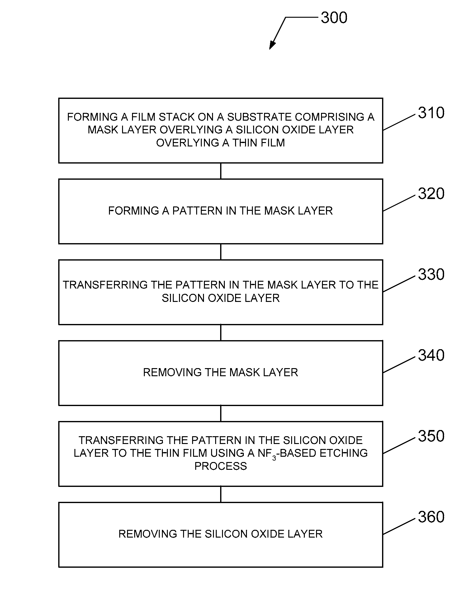
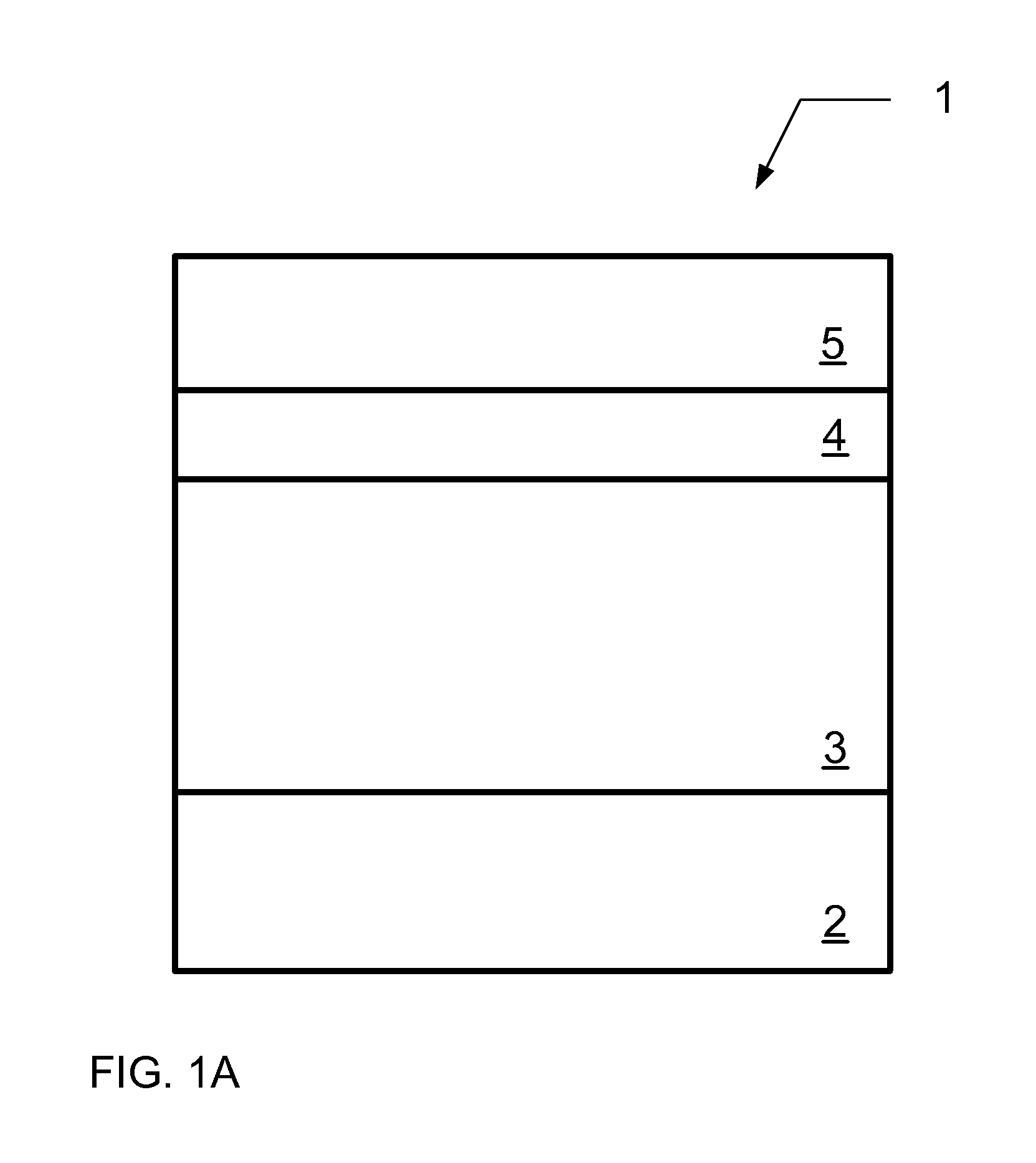
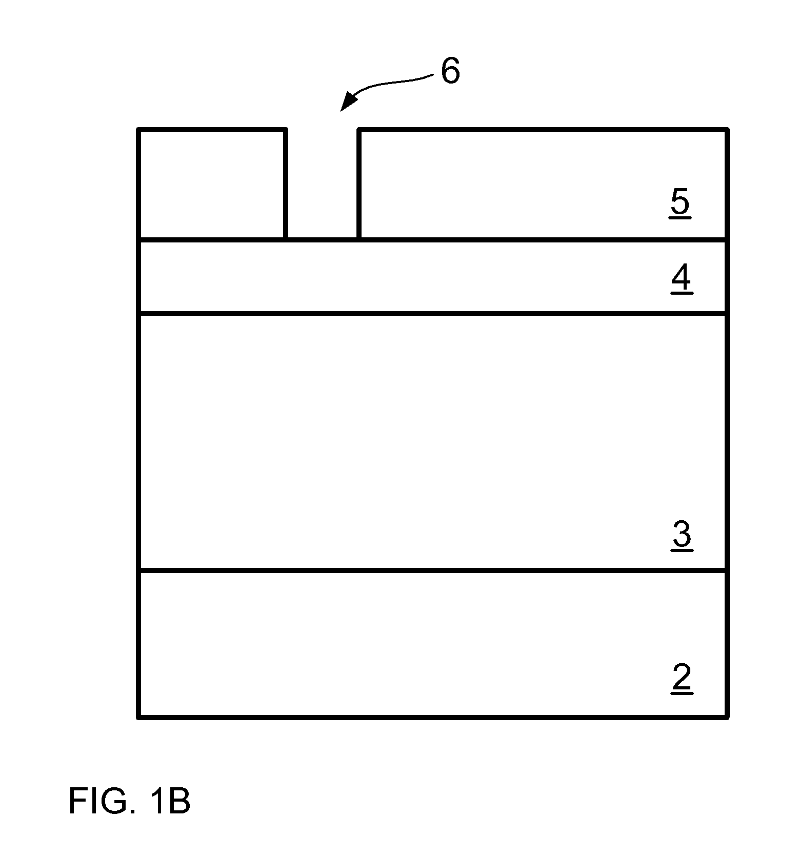
[0024]According to one embodiment, a method of patterning a film stack is described. The method comprises preparing a film stack on a substrate, wherein the film stack comprises a SiCOH-containing layer formed on the substrate, a silicon oxide (SiOx) layer formed on the SiCOH-containing layer, and a mask layer formed on the silicon oxide layer. A pattern is created in the mask layer. Thereafter, the pattern in the mask layer is transferred to the silicon oxide layer using an etching process, and then the mask layer is removed. The pattern in the silicon oxide layer is transferred to the SiCOH-containing layer using a dry plasma etching process formed from a process composition comprising N...


PUM


Abstract

A method of patterning a film stack is described. The method comprises preparing a film stack on a substrate, wherein the film stack comprises a SiCOH-containing layer formed on the substrate, a silicon oxide (SiOx) layer formed on the SiCOH-containing layer, and a mask layer formed on the silicon oxide layer. A pattern is created in the mask layer. Thereafter, the pattern in the mask layer is transferred to the silicon oxide layer using a first etching process, and then the mask layer is removed. The pattern in the silicon oxide layer is transferred to the SiCOH-containing layer using a second etching process formed from a process composition comprising NF3. Thereafter, the silicon oxide layer is removed using a third etching process.

Description

CROSS-REFERENCE TO RELATED APPLICATIONS[0001]This application is related to pending U.S. patent application Ser. No. 11 / 836,957, entitled “METHOD FOR ETCHING LOW-K MATERIAL USING AN OXIDE HARD MASK” (TTCA-223), filed on Aug. 10, 2007; and pending U.S. patent application Ser. No. 11 / 836,977, entitled “METHOD FOR FORMING A DAMASCENE STRUCTURE” (TTCA-226), filed on Aug. 10, 2007. The entire contents of these applications are herein incorporated by reference in their entirety.BACKGROUND OF THE INVENTION[0002]1. Field of the Invention[0003]The present invention relates to a method for metallizing a pattern in a low dielectric constant (low-k) dielectric film on a substrate, and more particularly to a method for metallizing a dual damascene structure in a SiCOH-containing low-k film.[0004]2. Description of Related Art[0005]In material processing methodologies, pattern etching can comprise the application of a thin layer of radiation-sensitive material, such as photoresist, to an upper sur...

Claims


Application Information

Patent Timeline
IPC IPC(8): H01L21/311
CPCH01L21/31144H01L21/76814H01L21/76813H01L21/76811
Inventor FEURPRIER, YANNICK
Owner TOKYO ELECTRON LTD
Why Eureka
Try Eureka