Method of manufacturing substrate for liquid discharge head

a technology of liquid discharge head and substrate, which is applied in the direction of recording equipment, instruments, and recording information storage, etc., can solve the problems of inability to manufacture miniaturized ink supply openings, difficult to deeply dig si with accuracy, and limited miniaturization of chip substrates, etc., to achieve the effect of forming with accuracy and stability

Inactive Publication Date: 2009-03-12
CANON KK
View PDF13 Cites 15 Cited by
  • Summary
  • Abstract
  • Description
  • Claims
  • Application Information

AI Technical Summary

Benefits of technology

[0015]Accordingly, the present invention is made to solve the problems of the above-mentioned related arts. An object of the present invention is to provide a method of forming with accuracy and stability an ink supply opening which can achieve miniaturization of a substrate for an ink jet head.

Problems solved by technology

However, in order to form the through opening, this method requires a large opening width in the mask on the back surface.
Thus, in a method of forming an ink supply opening of this kind, the size of the chip substrate is defined by the size of the ink supply opening, and hence miniaturization of the chip substrate is limited.
However, with regard to a substrate for an ink jet head in which, after wiring and nozzles are formed on a surface of the substrate, the blind trench is formed and anisotropic etching is performed from a back surface of the substrate to form the through opening, the following problem arises.
Specifically, taking into consideration damage of the substrate and stability of the depth of the processing, it is difficult to deeply dig Si with accuracy, and a miniaturized ink supply opening cannot be manufactured.
In U.S. Pat. No. 6,648,454, sandblasting, dicing, dry etching, and laser processing are listed as exemplary methods of processing Si, but those methods cannot be adapted for deeply digging Si in manufacturing the above-mentioned substrate for an ink jet head for the following reasons.
First, machining such as sandblasting or dicing generates various sizes of cracks, which causes more chipping and cracks of the substrate.
Second, dry etching has a low etching rate, and hence is less productive and is not a realistic method.
With regard to laser processing, Si removed in the processing (hereinafter, referred to as debris) accumulates at the bottom of and on an end face of the processed hole to cause scattering of an entering laser, which makes it difficult to deeply dig Si.
However, in this case, the increased spot diameter decreases irradiated energy per unit area, and hence the processing ability is lowered.
However, since the processing energy is too high, it becomes considerably difficult to control the depth of the processed hole.
In that case, a further problem arises that wiring and nozzles already formed on the surface of the substrate are damaged to spoil the function as an ink jet head.

Method used


Image

  • Method of manufacturing substrate for liquid discharge head
  • Method of manufacturing substrate for liquid discharge head
  • Method of manufacturing substrate for liquid discharge head

Examples


first embodiment

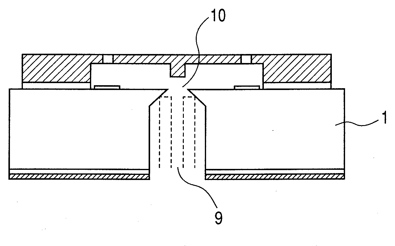
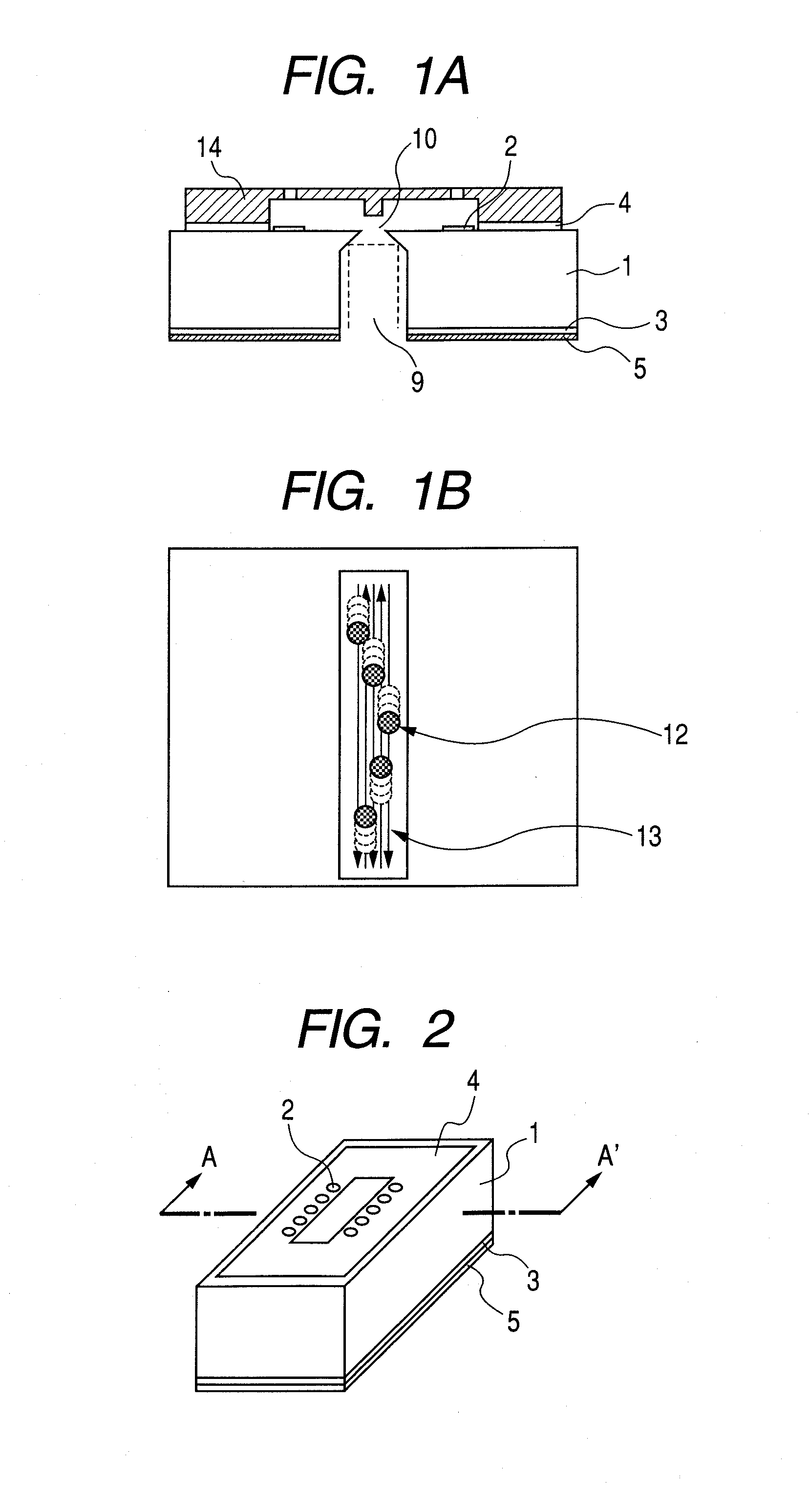
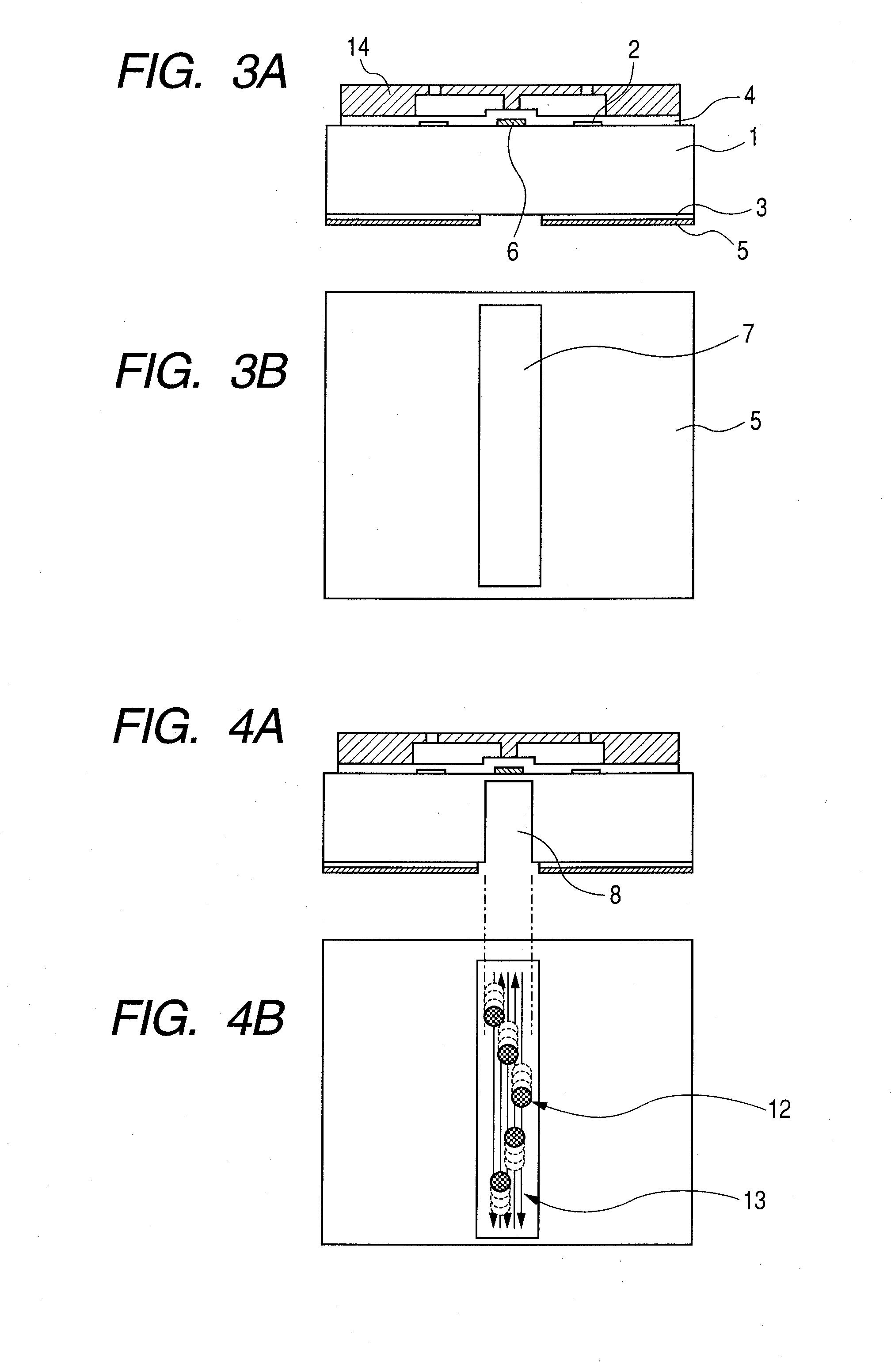
[0028]FIG. 1A is a sectional view of an ink jet head using a substrate for an ink jet head according to a first embodiment of the present invention, and FIG. 1B is a bottom view of the ink jet head. FIG. 2 is a perspective view of the substrate for an ink jet head according to the first embodiment, FIG. 3A is a sectional view taken along the line A-A′ illustrated in FIG. 2, and FIG. 3B is a bottom view of the substrate illustrated in FIGS. 1A and 1B.

[0029]With reference to those figures, the ink jet head is formed by forming a flow path formation layer 14 on a front surface side of the substrate for an ink jet head. The flow path formation layer 14 has an ink flow path 10 enclosing ink discharge energy generating elements 2 and liquid discharge openings disposed so as to be opposed to the ink discharge energy generating elements 2, respectively. Further, an ink supply opening 9 as a through opening which is formed so as to pierce the substrate from a back surface side of the substra...

second embodiment

[0039]Next, a method of manufacturing a substrate for an ink jet head according to a second embodiment is described. FIGS. 6A, 6B and 7 illustrate a method of laser ablation for achieving the manufacturing method according to the second embodiment. It is to be noted that FIGS. 6A and 7 are sectional views taken along the line A-A′ illustrated in FIG. 2 and illustrates states of a processed ink supply opening.

[0040]With reference to those figures, wiring (not shown) made of Al or the like and a plurality of ink discharge energy generating elements 2 made of a high resistance material such as TaSiN or TaN are formed in two lines on one side of the silicon substrate 1. Then, an insulation protection film 4 made of SiN or the like is formed so as to cover the upper portion of the wiring and the ink discharge energy generating elements 2. The insulation protection film 4 protects the wiring structure on the substrate 1 from ink and liquid, and also functions as an etching stop layer when...


PUM

PropertyMeasurementUnit
thicknessaaaaaaaaaa
thicknessaaaaaaaaaa
thicknessaaaaaaaaaa

Abstract

Provided is a method of manufacturing a substrate for a liquid discharge head, the substrate including a silicon substrate with a liquid supply opening formed therein, the method including: forming one processed portion by laser processing on the substrate from one surface of the substrate; expanding the one processed portion to form a recess portion by performing laser processing at a position which overlaps a part of the one processed portion and does not overlap another part of the one processed portion; and etching from the one surface the substrate with the recess portion formed therein to form the liquid supply opening.

Description

BACKGROUND OF THE INVENTION[0001]1. Field of the Invention[0002]The present invention relates to a method of manufacturing a substrate for a liquid discharge head used for a liquid discharge head.[0003]2. Description of the Related Art[0004]As a liquid discharge head for discharging liquid, an ink jet head for discharging ink being liquid is known. In a typical ink jet head, a through opening (ink supply opening) is provided in a substrate having an ink discharge pressure generating elements formed thereon, and the ink is supplied from a surface opposite to a surface having the ink discharge pressure generating elements formed thereon.[0005]As a method of forming an ink supply opening of this type, U.S. Pat. No. 6,143,190 proposes a method in which a silicon substrate with a patterned mask material is anisotropically etched in a strong alkaline solution. The gist of this method is to form an ink supply opening, the inner walls of which are all (111) surfaces, in a silicon substrate ...

Claims


Application Information

Patent Timeline
Patent Type & Authority Applications(United States)
IPC IPC(8): B44C1/22
CPCB41J2/1603B41J2/1628B41J2/1639B41J2/1631B41J2/1634B41J2/1629
Inventor KOMIYAMA, HIROTOKOMURO, HIROKAZUIBE, SATOSHIHATSUI, TAKUYAKISHIMOTO, KEISUKEASAI, KAZUHIROOTAKA, SHIMPEI
Owner CANON KK
Why Eureka
Try Eureka