
Semiconductor memory device with normal and over-drive operations

Active Publication Date: 2009-03-12
SK HYNIX INC
View PDF15 Cites 0 Cited by
  • Summary
  • Abstract
  • Description
  • Claims
  • Application Information

AI Technical Summary

Benefits of technology

[0017]There is provided a semiconductor memory device capable of preventing level fluctuation of a normal drive voltage due to over-driving.
[0018]There is also provided a semiconductor memory device capable of maintaining a predetermined node as a target level of normal driving during a normal driving interval after over-driving at the node.
[0019]There is also provided a semiconductor memory device capable of reducing time and costs due to the level adjustment of the normal drive voltage by appropriately discharging a level increment of the normal drive voltage due to over-driving.

Problems solved by technology

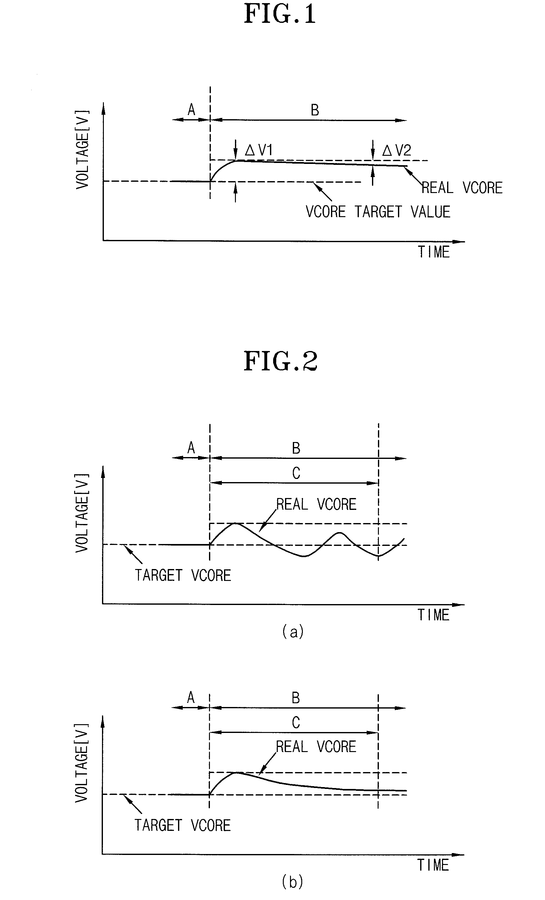
However, its discharge effect is extremely insignificant, and therefore, discharge is made by ΔV2 smaller than ΔV1.
However, in the conventional discharge circuit having such a configuration, since the discharge amount of the core voltage VCORE is determined depending on the size of the pull-down transistor, it is difficult to uniformly maintain the core voltage VCORE as the target level.
Current consumption may also be increased.
These problems may be improved through size tuning of the pull-down transistor, discharge time tuning of the core voltage and response speed tuning of the discharge circuit in failure analysis, which may result in increased time and costs.
The aforementioned problems frequently occur because an amount of over-driving current is changed corresponding to the level fluctuation of a power voltage VDD.

Method used


Image

  • Semiconductor memory device with normal and over-drive operations
  • Semiconductor memory device with normal and over-drive operations
  • Semiconductor memory device with normal and over-drive operations

Examples


Embodiment Construction

[0059]Hereinafter, preferred embodiments of the present invention will be described in detail with reference to the accompanying drawings.

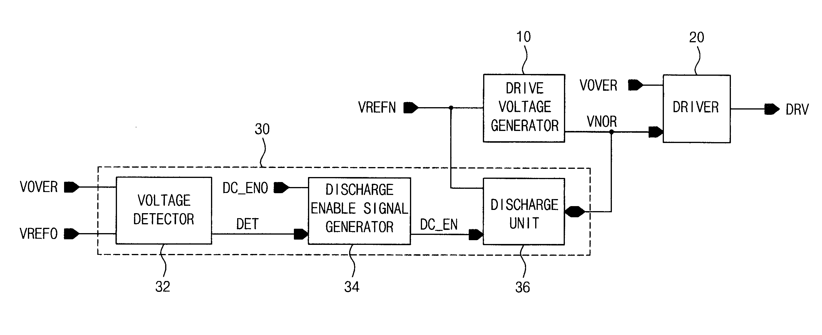
[0060]The present invention has a configuration in which, when over-driving and normal driving are consecutively performed, the discharge amount of a normal drive voltage is appropriately adjusted depending on the voltage level of an over-drive voltage by sensing the over-drive voltage, so that the normal drive voltage can be maintained as a target level at a normal driving interval.

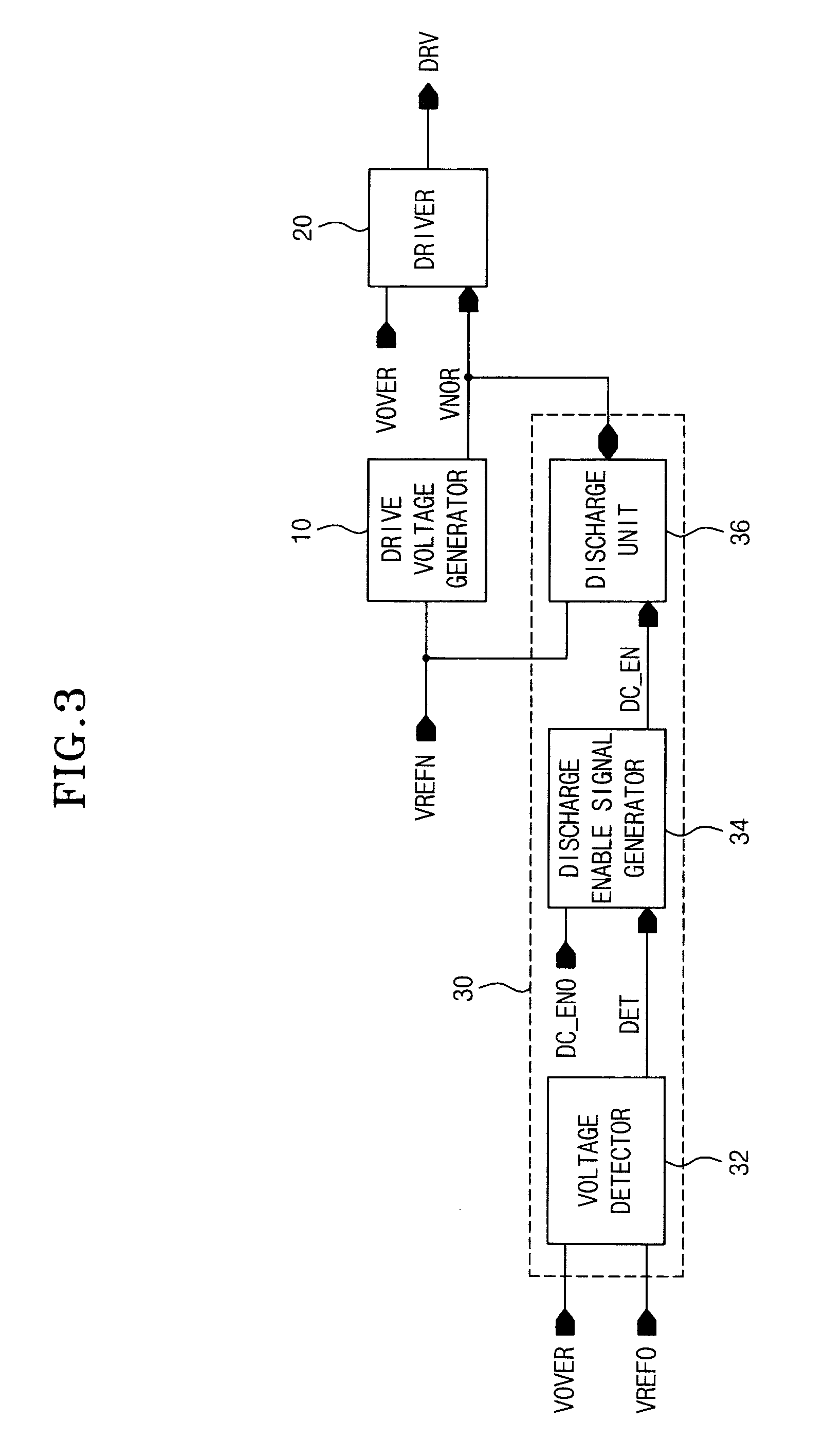
[0061]Specifically, referring to FIG. 3, a semiconductor memory device according to the present invention includes a drive voltage generator 10, a driver 20 and a drive voltage adjuster 30.

[0062]The drive voltage generator 10 generates a normal drive voltage VNOR corresponding to a reference voltage VREFN using the reference voltage VREFN having a target level of normal driving. Here, the normal drive voltage VNOR is an internal voltage, which may correspond to a core ...


PUM


Abstract

A semiconductor memory device having a driver configured to sequentially perform over-driving and normal driving operations is presented. The semiconductor memory device includes a driver that outputs a drive signal, that over-drives the drive signal with an over-drive voltage having a voltage level higher than a normal drive voltage, and then subsequently normally drives the drive signal with the normal drive voltage. The semiconductor memory device also includes a drive voltage adjuster that detects a level of the over-drive voltage and compensates for a change in the voltage level of the normal drive voltage in response to the detected level of the over-drive voltage.

Description

CROSS-REFERENCE TO RELATED APPLICATIONS[0001]The present application claims priority to Korean patent application number 10-2007-0091765 filed on Sep. 10, 2007, which is incorporated herein by reference in its entirety.BACKGROUND OF THE INVENTION[0002]The present invention relates to a semiconductor memory device, and more precisely to a semiconductor memory device including a driver sequentially performing over-driving and normal driving operations.[0003]In general, in a semiconductor memory device, when it is necessary to raise a predetermined node to a target level as quickly as possible, a method of over-driving the node higher than the target level in an initial operation is often used.[0004]As an example, a sensing amplifier sensing a bit line pair amplifies the bit line pair with drive voltages respectively supplied from a pull-up drive node and a pull-down drive node. Conventionally, in order to rapidly sense and amplify a bit line pair, a voltage of a level higher than a co...

Claims


Application Information

Patent Timeline
IPC IPC(8): G11C7/12
CPCG11C7/06G11C2207/065G11C7/08G11C5/14
Inventor BYEON, SANG JIN
Owner SK HYNIX INC
Learn More