Method for manufacturing semiconductor device and its manufacturing method

Inactive Publication Date: 2009-03-12
SEIKO EPSON CORP
View PDF6 Cites 20 Cited by
  • Summary
  • Abstract
  • Description
  • Claims
  • Application Information

AI Technical Summary

Benefits of technology

[0022]As a result, as described above, the first interlayer dielectric films on the plurality of ferroelectric capacitors can be formed in a uniform thickness, such that the plural connection holes can be formed

Problems solved by technology

However, in the ferroelectric memory devices, shapes of the contact holes may vary, and therefore differences in the characteristic may occur among the ferroelectric capacitors.
However, due to differences in the polishing amount which originate from unevenness in the base layer, differences in the thickness appear in the interlayer dielectric film.
Therefore, when the interlayer dielectric film is etched, the amount of etching becomes excessively small in thicker portions, and the amount of etching becomes excessively large in thinner portions of the interlayer dielectric film.
Such differences in the shape of the bottom portions of the contact holes mak

Method used


Image

  • Method for manufacturing semiconductor device and its manufacturing method
  • Method for manufacturing semiconductor device and its manufacturing method
  • Method for manufacturing semiconductor device and its manufacturing method

Examples


Embodiment Construction

[0028]An embodiment of the invention is described below with reference to the accompanying drawings. However, it should be noted that the technical scope of the invention is not limited to the embodiment described below. Also, it should be noted that, although various structures may be exemplified in the following description, using the accompanying drawings, the measurement and scale of each of the components of the structures illustrated in each of the drawings may be appropriately changed with respect to the actual structures so that characteristic features of each of the structures can be readily recognized.

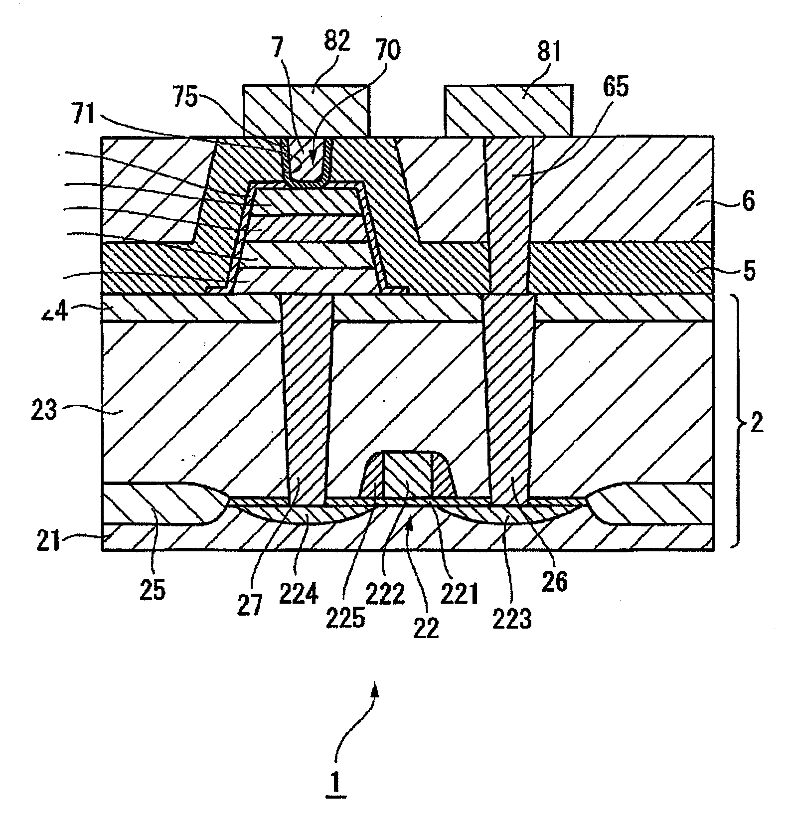
[0029]FIG. 1 is a side cross-sectional structural view of a portion of a semiconductor device (ferroelectric memory device) 1 in accordance with an embodiment of the invention. The ferroelectric memory device 1 may be equipped with a plurality of memory cells, but only one of them is illustrated in an enlarged view in FIG. 1. As shown in FIG. 1, the ferroelectric memory devic...


PUM


Abstract

A method for manufacturing a semiconductor device includes the steps of: forming a ferroelectric capacitor having a first electrode, a ferroelectric film and a second electrode successively laminated on a base substrate; forming a first interlayer dielectric film that covers the ferroelectric capacitor and the base substrate; forming a material film for a second interlayer dielectric film covering the first interlayer dielectric film; exposing the first interlayer dielectric film located on the ferroelectric capacitor by polishing an upper surface side of the material film for the second interlayer dielectric film by a CMP method; forming a contact hole that penetrates the first interlayer dielectric film and exposes the second electrode, after the step of exposing the first interlayer dielectric film; and forming in the contact hole a plug conductive section that conductively connects to the second electrode, wherein the first interlayer dielectric film has a lower polishing rate in the CMP method compared to the second interlayer dielectric film.

Description

[0001]The entire disclosure of Japanese Patent Application No. 2007-233877 filed Sep. 10, 2007 is expressly incorporated by reference herein.BACKGROUND[0002]1. Technical Field[0003]The present invention relates to methods for manufacturing semiconductor devices, and also relates to methods for manufacturing the same.[0004]2. Related Art[0005]Ferroelectric memory devices (FeRAM) are nonvolatile memory devices capable of low voltage and high speed operations, and their memory cells can be each formed from one transistor and one capacitor (1T / 1C). Accordingly, ferroelectric memory devices can achieve integration at the same level of that of DRAM, and are therefore expected as large-capacity nonvolatile memories.[0006]As the structures of such ferroelectric memory devices, a planer type (see, for example, Japanese laid-open patent application JP-A-2003-347512), a stacked type and the like may be enumerated. A ferroelectric memory device in any of the structures described above is equipp...

Claims


Application Information

Patent Timeline
IPC IPC(8): H01L21/00
CPCH01L21/76804H01L28/55H01L27/11507H01L21/7687H10B53/30
Inventor NODA, TAKAFUMI
Owner SEIKO EPSON CORP
Why Eureka
Try Eureka