Method for increasing the area of non-polar and semi-polar nitride substrates

Active Publication Date: 2009-03-19
RGT UNIV OF CALIFORNIA
View PDF11 Cites 12 Cited by
  • Summary
  • Abstract
  • Description
  • Claims
  • Application Information

AI Technical Summary

Benefits of technology

[0011]To overcome the limitations in the prior art described above, and to overcome other limitations that will become apparent upon reading and understanding the present specification, the present invention describes a technique for the production of large area and hig

Problems solved by technology

However, conventional c-plane quantum well structures in III-nitride based optoelectronic and electronic devices suffer from the undesirable quantum-confined Stark effect (QCSE), due to the existence of strong piezoelectric and spontaneous polarizations.
The strong built-in electric fields along the c-direction cause spatial separation of electrons and holes that in turn give rise to restricted carrier recombination efficiency, reduced oscillator strength, and red-shifted emission.
Unfortunately, in s

Method used


Image

  • Method for increasing the area of non-polar and semi-polar nitride substrates
  • Method for increasing the area of non-polar and semi-polar nitride substrates
  • Method for increasing the area of non-polar and semi-polar nitride substrates

Examples


example 1

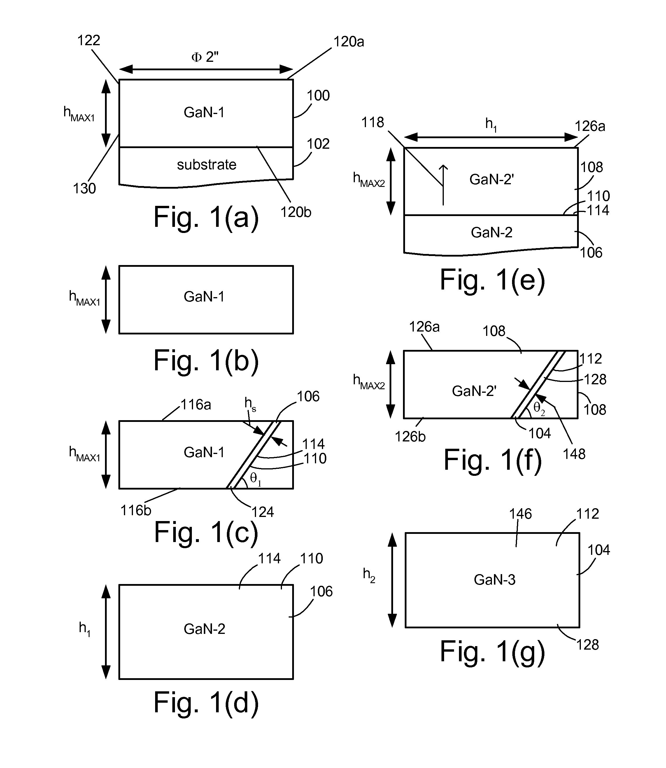
[0037]FIGS. 1(a)-(g) illustrate the process steps according to a preferred embodiment of the present invention. These process steps comprise the following:

[0038]1. Thick c-plane GaN growth (GaN-1) 100, to a thickness of hMAX1, on a substrate 102, as shown in FIG. 1(a), wherein Φ is the 2 inch diameter of the GaN-1 wafer 100.

[0039]2. Substrate 102 removal, leaving a thickness hMAX1 of c-plane GaN-1 100, as shown in FIG. 1(b).

[0040]3. Slicing a film 124 out of the c-plane GaN-1 100 along a semipolar plane 110 and at an angle θ1, as shown in FIG. 1(c), to form a sliced semipolar substrate GaN-2 106 having a surface 114 which is a semipolar plane 110 of width h1=hMAX1 / sin θ1, as shown by FIG. 1(d) which is the top view of the sliced semipolar substrate GaN-2 106.

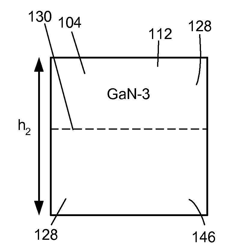
[0041]4. Growing a thickness hMAX2 of semipolar GaN on the surface 114 of GaN-2 106 to form a semipolar growth GaN-2′108 (i.e. growth in a semipolar direction 118 to achieve top surface 126a and bottom surface 126b of the GaN 10...

example 2

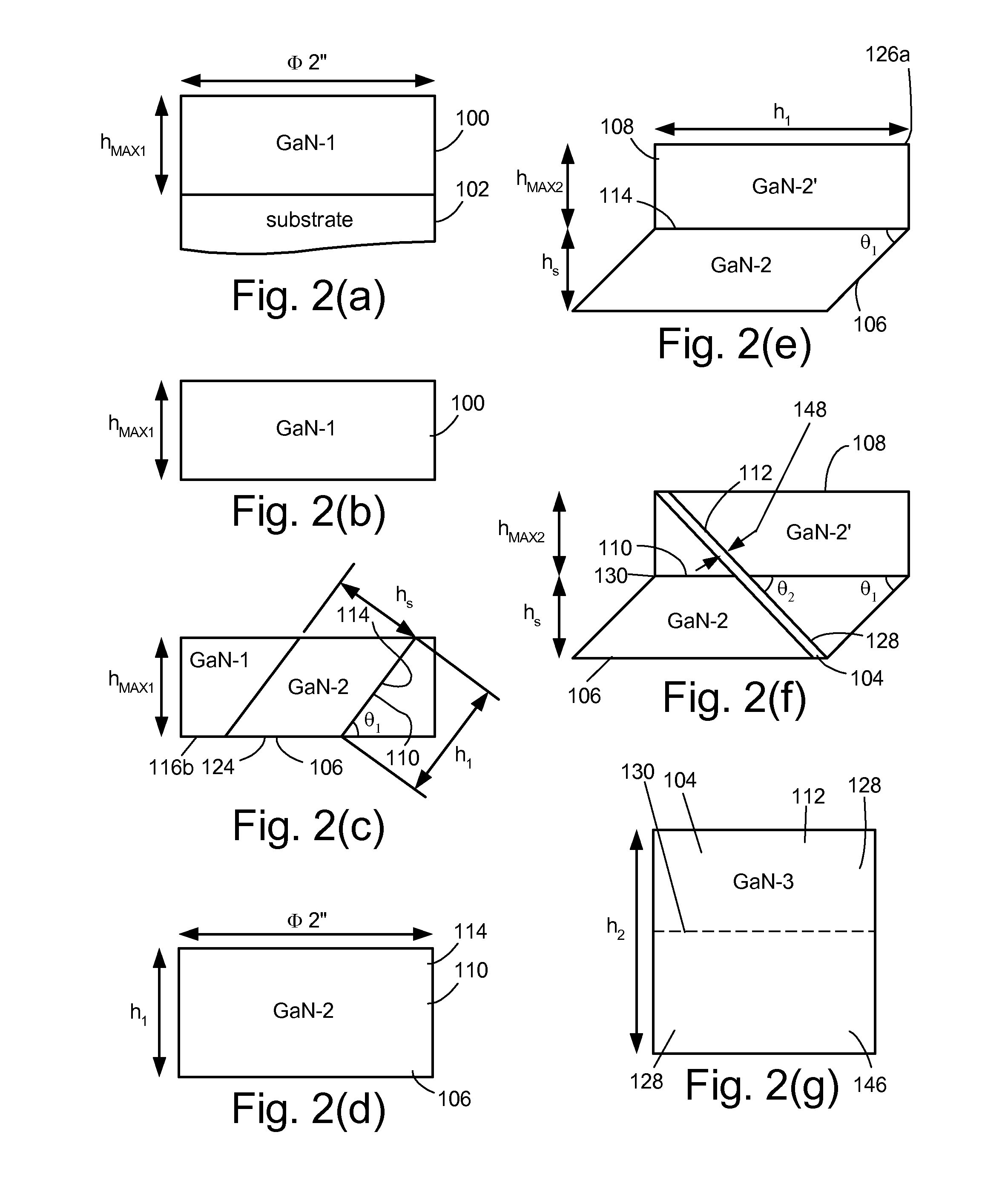
[0045]FIGS. 2(a)-(g) also illustrate the process steps according to a preferred embodiment of the present invention. These process steps comprise the following:

[0046]1. Thick c-plane GaN growth (GaN-1) 100, to a thickness of hMAX1, on a substrate 102, as shown in FIG. 2(a).

[0047]2. Substrate 102 removal, leaving a thickness hMAX1 of c-plane GaN-1 100, as shown in FIG. 2(b).

[0048]3. Slicing a film 124 out of the c-plane GaN-1 100 along a semipolar plane 110 at an angle θ1, as shown in FIG. 2(c), to form a sliced semipolar substrate GaN-2 106 having a surface 114 that is a semipolar plane 110 of width h1=hMAX1 / sin θ1, as shown in FIG. 2(d), which is a top view of the sliced semipolar substrate GaN-2 106. The sliced semipolar substrate GaN-2 106 has a height hS.

[0049]4. Growing a thickness hMAX2 of semipolar GaN on the surface 114 (which is a semipolar plane 110) of GaN-2 106 to form a semipolar growth GaN-2′108 (growth along a semipolar direction 118 to achieve top surface 126a which ...


PUM


Abstract

A method for fabricating a high quality freestanding nonpolar and semipolar nitride substrate with increased surface area, comprising stacking multiple films by growing the films one on top of each other with different and non-orthogonal growth directions.

Description

CROSS-REFERENCE TO RELATED APPLICATIONS[0001]This application claims the benefit under 35 U.S.C. Section 119(e) of co-pending and commonly-assigned U.S. Provisional Patent Application Ser. No. 60 / 973,656, filed on Sep. 19, 2007, Asako Hirai, James S. Speck, Steven P. DenBaars, and Shuji Nakamura, entitled “METHOD FOR INCREASING THE AREA OF NONPOLAR AND SEMIPOLAR NITRIDE SUBSTRATES” attorneys' docket number 30794.242-US-P1 (2007-675-1), which application is incorporated by reference herein.BACKGROUND OF THE INVENTION[0002]1. Field of the Invention[0003]This invention relates to a technique for the production of large area, high quality freestanding (FS) nonpolar and semipolar nitride substrates.[0004]2. Description of the Related Art[0005]The usefulness of gallium nitride (GaN), and its ternary and quaternary compounds incorporating aluminum and indium (AlGaN, InGaN, AlInGaN), has been well established for fabrication of visible and ultraviolet optoelectronic devices and high-power e...

Claims


Application Information

Patent Timeline
IPC IPC(8): H01L21/20H01L29/20
CPCC30B29/403C30B33/00H01L21/02389H01L29/2003H01L21/0254H01L21/02658H01L21/02433
Inventor HIRAI, ASAKOSPECK, JAMES S.DENBAARS, STEVEN P.NAKAMURA, SHUJI
Owner RGT UNIV OF CALIFORNIA
Why Eureka
Try Eureka