Organic electroluminescent apparatus and elctronic appratus

Inactive Publication Date: 2009-03-19
SEIKO EPSON CORP
View PDF3 Cites 32 Cited by
  • Summary
  • Abstract
  • Description
  • Claims
  • Application Information

AI Technical Summary

Benefits of technology

[0010]An advantage of some aspects of the invention is that it provides an organic EL apparatus and an

Problems solved by technology

Characteristics of organic thin films included in organic EL devices are easily altered and deteriorated by oxygen or moisture.
Such alteration and deterioration of characteristics shortens the lifetime of organic EL devices.
However, it takes time before organic thin films provided in a central region of the element area start to be deteriorated.
This means that, while light-emitting elements in the central region are still capable of emitting light, light-emitting elements in the peripheral region may become incapable of emitting light.
In such an event, an organic EL apparatus itself becomes unusable (a first problem).
Such nonuniformity in the drying rate often triggers nonuniformity in the thickness of organic thin films to be formed.
Further, nonuniformity in the thickness of organic thin films often triggers nonuniformity in the brightness

Method used


Image

  • Organic electroluminescent apparatus and elctronic appratus
  • Organic electroluminescent apparatus and elctronic appratus
  • Organic electroluminescent apparatus and elctronic appratus

Examples


first embodiment

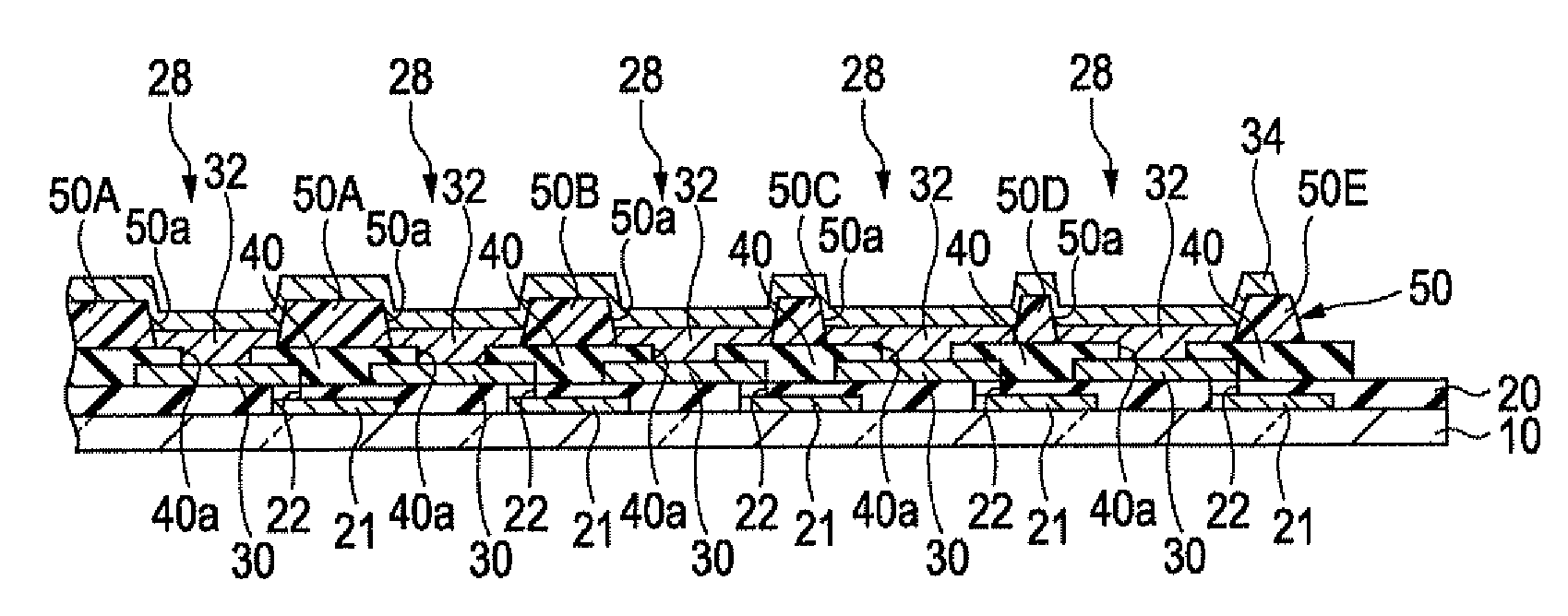
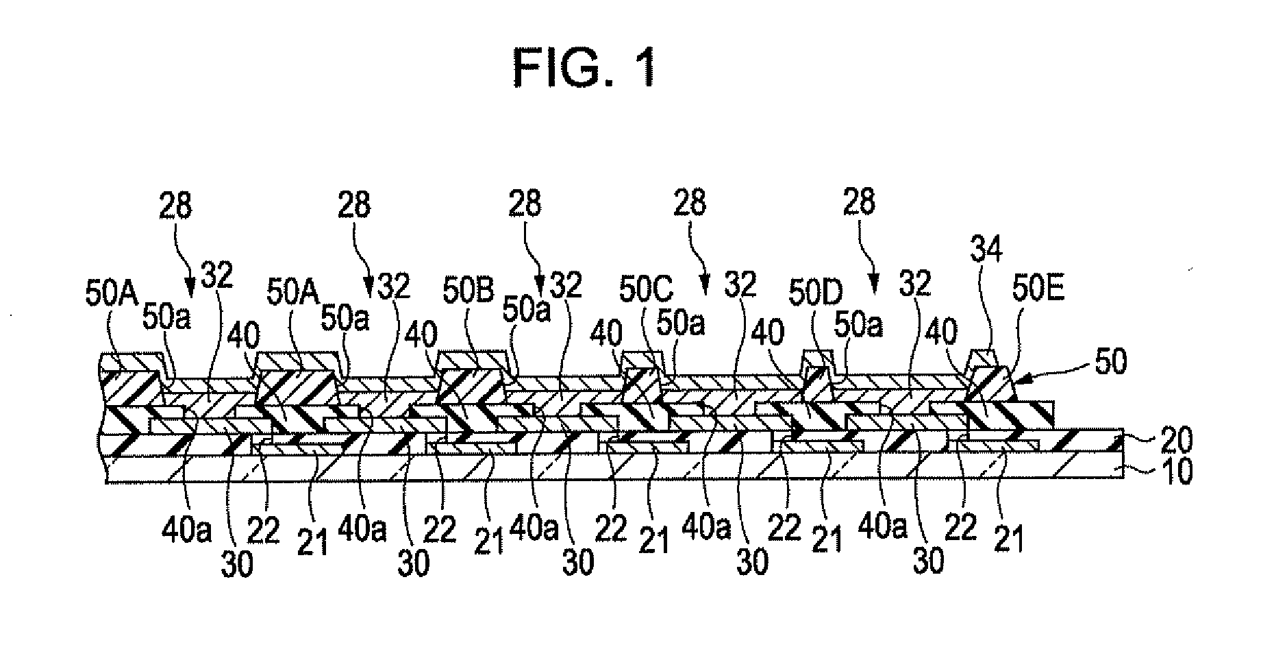
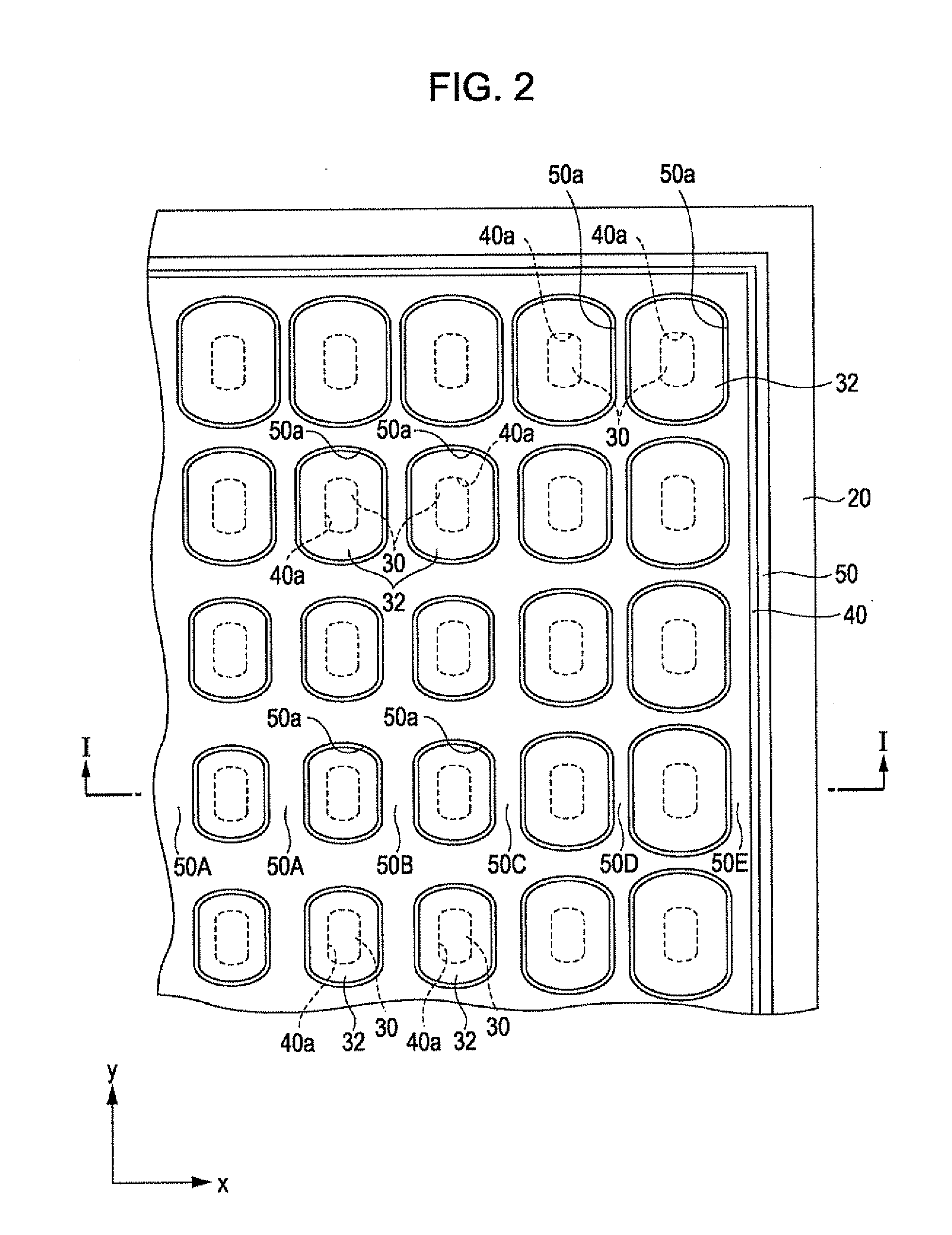
[0035]FIG. 1 is a cross-sectional view of an organic EL apparatus according to a first embodiment of the invention. FIG. 2 is a plan view of the organic EL apparatus without a counter electrode 34. More specifically, FIG. 1 is a cross-sectional view taken along the line I-I in FIG. 2.

[0036]Referring to FIG. 1, the organic EL apparatus includes a substrate 10 and an insulator layer 20 disposed on the substrate 10. The insulator layer 20 is composed of silicon oxide or silicon nitride, for example. A plurality of thin film transistors (TFTs) 21 and wires (not shown) for supplying power to a plurality of light-emitting devices (organic EL devices) 28 are embedded in the insulator layer 20.

[0037]The light-emitting elements 28 are provided on the insulator layer 20. Each of the light-emitting elements 28 includes a positive electrode, a negative electrode, and an organic layer (organic thin film) held therebetween. More specifically, the light-emitting element 28 includes an individual p...

second embodiment

[0063]FIGS. 7A to 7D are cross-sectional views of a color filter panel showing a method for manufacturing a color filter panel according to a second embodiment of the invention. FIG. 8 is a plan view of the color filter panel as a finished product. More specifically, FIGS. 7A to 7D are each a cross-sectional view taken along the line VII-VII in FIG. 8. The color filter panel includes a substrate 100 composed of a transparent material such as glass or transparent resin, color filters 104 (104R, 104G, and 104B) provided on the substrate 100, and a bank pattern (partition pattern) provided on the substrate 100 and defining the color filters 104. The suffixes R, G, and B given to the color filters 104 indicate colors of light that are transmitted through the respective color filters 104. Namely, the color filters 104R transmit red light, the color filters 104G transmit green light, and the color filters 104B transmit blue light.

[0064]The bank pattern has a two-layer structure including ...


PUM


Abstract

An organic electroluminescent apparatus includes a plurality of light-emitting elements each having an organic layer held between a pixel electrode and a counter electrode, and a partition pattern with which the organic layers of the individual light-emitting elements are defined. The partition pattern has a plurality of openings in which the organic layers are respectively provided, the plurality of openings including first openings provided in a peripheral region of a element area, in which the light-emitting elements are arranged, and second openings provided in a region closer to the center of the element area than the region where the first openings are provided. The first openings have larger planar dimensions than those of the second openings.

Description

BACKGROUND[0001]1. Technical Field[0002]The present invention relates to organic electroluminescent apparatuses and electronic apparatuses.[0003]2. Related Art[0004]Organic light-emitting diodes (OLEDs), i.e., organic electroluminescent (EL) devices included in thin and light self-luminous displays are attracting attention. An organic EL device includes at least one organic thin film layer composed of an organic material and held between a pixel electrode and a counter electrode, as disclosed in JP-A-2002-252083, for example.[0005]Characteristics of organic thin films included in organic EL devices are easily altered and deteriorated by oxygen or moisture. Such alteration and deterioration of characteristics shortens the lifetime of organic EL devices. Deterioration of organic thin films tends to occur first in a peripheral region of a element area that easily allow entry of oxygen or moisture. However, it takes time before organic thin films provided in a central region of the elem...

Claims


Application Information

Patent Timeline
IPC IPC(8): H01J1/63
CPCH01L51/5284H01L27/3246H10K59/122H10K50/865
Inventor SEKI, SHUNICHIOTA, TSUKASA
Owner SEIKO EPSON CORP
Why Eureka
Try Eureka