Data management equipment used to defect review equipment and testing system configurations

a technology of data management equipment and defect review equipment, applied in the field of defect review equipment, can solve the problems of long inspection time and long time-consuming for the collection of necessary data, and achieve the effect of reducing inspection tim

Inactive Publication Date: 2009-03-19
HITACHI HIGH-TECH CORP
View PDF7 Cites 30 Cited by
  • Summary
  • Abstract
  • Description
  • Claims
  • Application Information

AI Technical Summary

Benefits of technology

[0005]As to related prior art: for a method of acquiring a defect image, it is proposed to make use of a scanning electron microscope (see, for example, JP-A-2000-30652); a defect review system is proposed in which a synthesized reference image free of defect is generated from a defect candidate image of a low magnification to reduce the number of times of imaging thereby shortening an inspection time (see, for example, JP-A-2007-40910); and an inspection system is proposed which includes a navigation system having design data for a semiconductor circuit such as CAD data stored therein and establishing, on the basis of the design data, imaging / inspection conditions including areas of a semiconductor wafer to be inspected and includes a scanning electron microscope carrying out size measurement / inspection (see, for example, JP-A-2002-328015).
[0008]An object of the present invention is to provide a data management equipment which enjoys a short inspection time even when a design data for a semiconductor circuit is utilized.
[0009]Another object of the invention is to provide a testing system which enjoys a short inspection time.
[0010]Another object of the invention is to provide a defect review system which enjoys a short inspection time.
[0017]In accordance with one or more of the above aspects of the present invention, the data management equipment, the testing system and / or the defect review system enjoy shortened inspection time even when use is made of semiconductor design data.

Problems solved by technology

However, the design data is so voluminous or big that retrieval of necessary data takes a long time, which may lead to a long inspection time.

Method used


Image

  • Data management equipment used to defect review equipment and testing system configurations
  • Data management equipment used to defect review equipment and testing system configurations
  • Data management equipment used to defect review equipment and testing system configurations

Examples


Embodiment Construction

[0044]Embodiments of the present invention will now be described in detail with reference to the accompanying drawings. In the drawings, same reference numerals are used to denote similar members and explanation of the similar members will not be repeated.

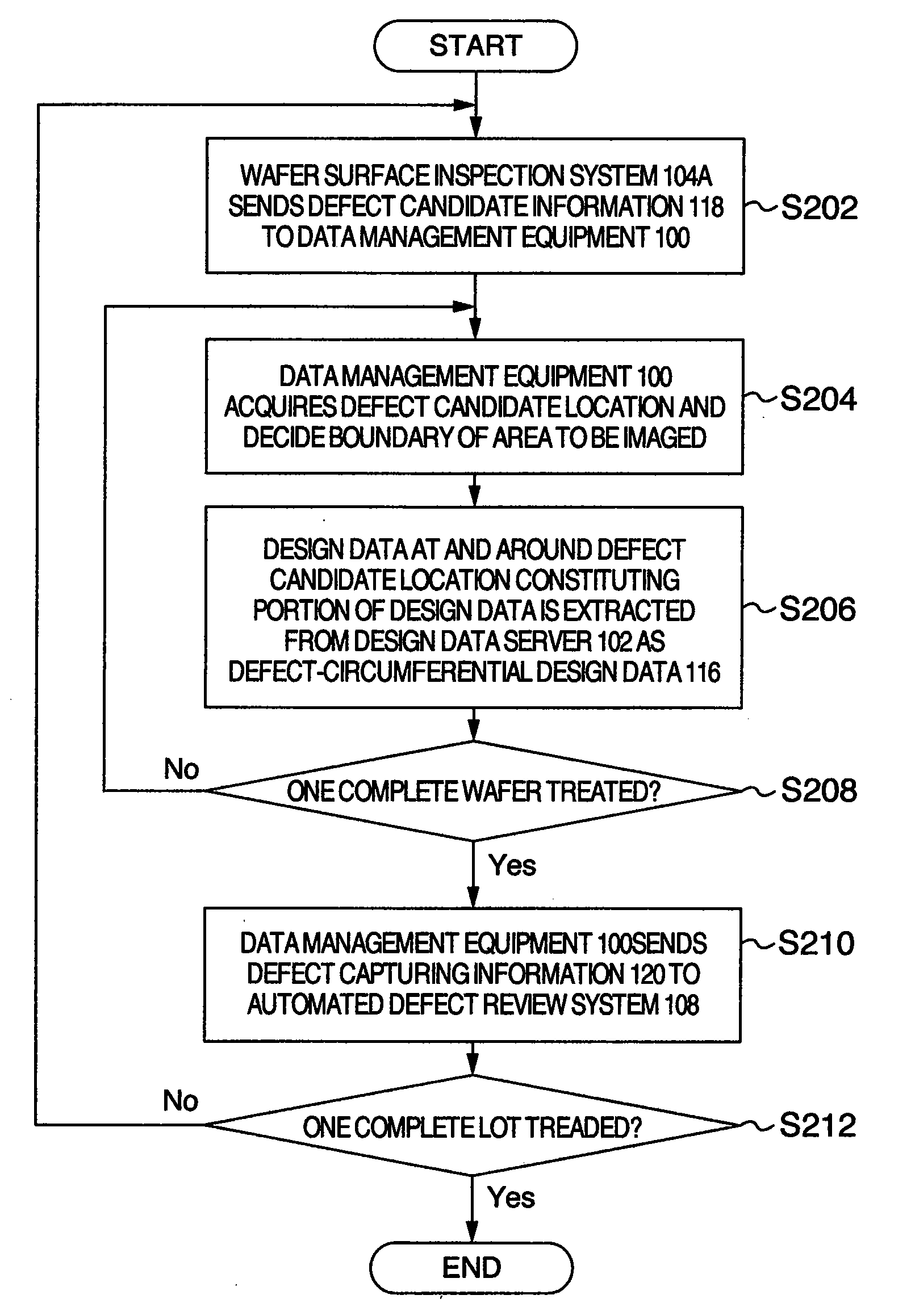
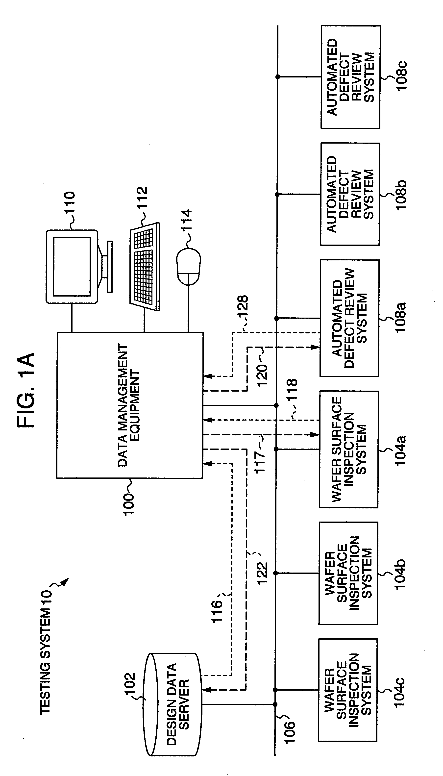
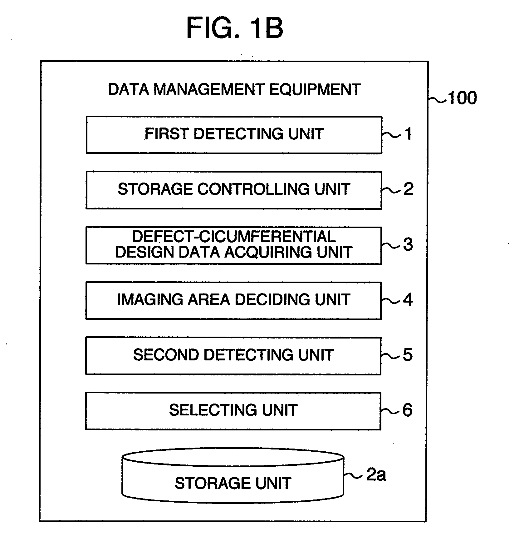
[0045]FIG. 1A is a structural diagram of a testing system 10 according to an embodiment of the present invention. A data management equipment 100, plural (automated) defect review systems 108a, 108b and 108c, a design data server 102, and plural general inspection systems or plural (wafer surface) inspection systems 104a, 104b and 104c are connected with one another through a network 106.

[0046]Each of the general inspection systems 104a, 104b and 104c detects candidates for defects on a wafer or an exposure mask used to manufacture semiconductor circuits and acquires a defect candidate location of each of the detected defect candidates. The inspection system 104a acquires a size of each of the defect candidates in accordance with t...


PUM

PropertyMeasurementUnit
defectaaaaaaaaaa
defect reviewaaaaaaaaaa
sizesaaaaaaaaaa

Abstract

A data management equipment connected with a general inspection system for detecting a defect candidate on a wafer and acquiring a location thereof, a design data server for storing a design data for a semiconductor circuit and a defect review system for acquiring a defect data image on the basis of the location and comparing the defect candidate image with a defect-free reference image to identify a defect. The data management equipment includes a first detecting unit for finding that the general inspection system is acquiring a location, a storage controlling unit responsive to the finding to start to store the location from the general inspection system in a storage unit and a defect-circumferential design data acquiring unit for acquiring from a portion of the design data a defect-circumferential design data such that a reference image including the location can be produced from the defect-circumferential design data.

Description

BACKGROUND OF THE INVENTION[0001]The present invention relates to defect review systems for identifying a plurality of defects on a wafer or an exposure mask used in the manufacturing of semiconductor circuits. The invention also relates to testing systems including such defect review system and to data management equipments connected with such defect review system.[0002]In the field of semiconductor circuits, the selling prices are being made lower, diversified small-quantity production is being promoted, and shorter time limit of delivery is being encouraged. Accordingly, it is now required in the process of manufacturing semiconductor circuits to enhance the production yield and to reduce the chip size by the use of the fine patterning techniques for reduction of the production cost. To this end, defects such as disconnection, shorts and contamination by foreign materials are discovered in respective manufacturing steps, and countermeasures have been developed against them.[0003]...

Claims


Application Information

Patent Timeline
Patent Type & Authority Applications(United States)
IPC IPC(8): G06K9/00G03F1/84H01L21/027H01L21/66
CPCG01N21/9501G01N21/956G06T2207/30148G06T7/0006G06T2207/10056G01N2021/8861
Inventor KITAZAWA, MASAHIROIKEDA, MITSUJI
Owner HITACHI HIGH-TECH CORP
Why Eureka
Try Eureka