Thin film transistor manufacturing method and substrate structure

a manufacturing method and substrate technology, applied in the direction of semiconductor devices, basic electric elements, electrical appliances, etc., can solve the problems of low yield, inaccurate alignment, and difficult to change the way people used to read, so as to improve the efficiency of backlighting

Inactive Publication Date: 2009-03-19
IND RES INST
View PDF3 Cites 4 Cited by
  • Summary
  • Abstract
  • Description
  • Claims
  • Application Information

AI Technical Summary

Benefits of technology

[0009]The invention provides a method of forming a self-alignment mask on the front or back surface of a substrate, where a self-alignment back exposure may proceed to expose the source, the drain or the gate. Accordingly, changing the mask design and driving system becomes unnecessary. Because the self-alignment mask is made by metal, using it to define the channel of the active layer can not only prevent the backlight from producing an optical current but can also reflect this backlight to the backlight system. Thus, the light is recycled and backlight efficiency can be improved.
[0015]1. The process yield can be improved. Because the alignment inaccuracy occurring when defining the source and the drain due to the substrate thermal expansion offset can be reduced by the self-alignment mask.
[0016]2. Backlight efficiency can be improved. Because a metal film or a metal oxide film is used as the self-alignment mask, when a light is provided from a backlight module it is reflected by the metal film to enhance lighting efficiency.
[0017]3. A better semiconductor property can be obtained. Because the alignment problem has been solved by this invention, a source and drain of a transistor therefore can be formed at the precise position as well as the active layer, and as a result all elements of the device are unified.
[0018]4. Cost can be reduced. The invention can not only improve the yield but can also prevent producing costs in manufacturing additional specific masks.

Problems solved by technology

However, the way people used to read is not easy to change; therefore paper still plays an important role as an information carrier.
However, there is not only the problem of how to improve the oxygen and water permeability of the substrate in the plastic substrate process, but also the problem of inaccurate alignment caused by the varied size of the substrate during solvent rinsing and high temperature process.
Thus, this process is difficult and causes a low yield.
These offsets may seriously affect the accuracy of the alignment and may further make the thin film transistors unstable or inconsistent if the inaccuracy problem is not solved.
Besides, because different types of plastic substrate have different extents of thermal expansion, it complicates the process and increases the cost if a different plastic substrate is applied every time and a different mask has to be provided.
Accordingly, changing the mask design and driving system becomes unnecessary.

Method used


Image

  • Thin film transistor manufacturing method and substrate structure
  • Thin film transistor manufacturing method and substrate structure
  • Thin film transistor manufacturing method and substrate structure

Examples


first embodiment

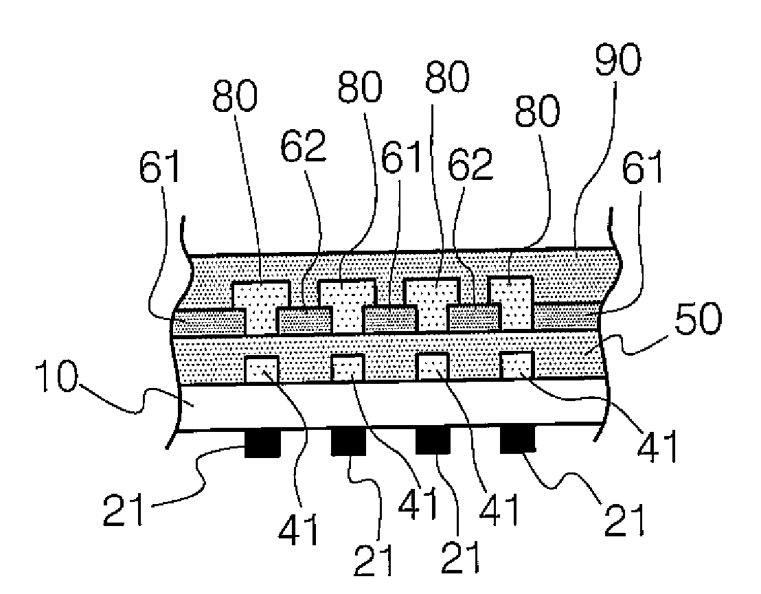
[0059]A TFT manufacturing method (M10) according to this embodiment is particularly suitable for a display having a backlight module. In order to enhance the backlight module's lighting efficiency, the TFT manufacturing method (M10) uses a first mask 21 which is complementary to the source 61 and the drain 62 of the TFT in position, measure of area and shape; and a negative type photo resist layer 70 to define the source 61 and the drain 62 of a TFT.

[0060]Please refer to FIG. 3A, which is a diagram showing a second surface of a substrate forming an opaque thin film thereon. In this embodiment, first provide a substrate 10 for manufacturing a TFT thereon. The substrate 10 has a first surface 11 and a second surface 12 on which is formed a transistor including a source 61, a drain 62, and a gate 41. Then the second surface 12, where no TFT forms, has an opaque thin film 20 forming thereon for manufacturing the first mask 21.

[0061]Please refer to FIG. 3B, which is a diagram showing a f...

second embodiment

[0067]A TFT manufacturing method (M20) according to this embodiment is particularly suitable for a reflective display. In order to increase the reflective area of the display, the TFT manufacturing method (M20) uses a second mask 22 which is the same with the source 61 and the drain 62 of the TFT in position, measure of area and shape; and a transparent gate 43 and a positive type photo resist layer 71 to define the source 61 and the drain 62 of a TFT.

[0068]Please refer to FIG. 5A, which is a diagram showing a second surface of a substrate forming an opaque thin film thereon. In this embodiment, first provide a substrate 10 for manufacturing a TFT thereon. The substrate 10 has a first surface 11 and a second surface 12. The first surface is used for forming a transistor including a source 61, a drain 62, and a transparent gate 43 formed thereon. Then the second surface 12, where not used to form TFT, has an opaque thin film 20 forming thereon for manufacturing the second mask 22.

[00...

third embodiment

[0075]A TFT manufacturing method (M30) according to this embodiment is particularly suitable for a display that has a backlight module. Like method M10, although this method is also for enhancing the backlight module's lighting efficiency, this method uses an opaque gate 45 as a gate electrode and a self-alignment mask for making the source 61 and the drain 62 at the same time. The opaque gate 45 works with a negative type photo resist layer 70 to define the source 61 and the drain 62 of a TFT.

[0076]Please refer to FIG. 7A, which is a diagram showing a first surface of a substrate forming an opaque gate thin film thereon. In this embodiment, first provide a substrate 10 for manufacturing a TFT thereon. Then an opaque gate thin film 44 is formed on one surface of the substrate 10.

[0077]Please refer to FIG. 7B, which is a diagram showing an opaque gate thin film processed to form the opaque gate by the photolithography process. First a photo resist layer 30 is formed on the opaque gat...


PUM


Abstract

A method of TFT (Thin Film Transistor) manufacturing and a substrate structure are provided. The structure includes a substrate and a self-alignment mask. A self-alignment mask on a substrate is first manufactured and then the self-alignment mask may synchronously extend with the substrate during the thermal process. When an exposure light source is provided on the side without a TFT formed, the self-alignment mask can overcome the problem that when a plastic substrate extends, the positions of the source and drain to be formed on the plastic substrate are incorrect, which has a great effect on the accuracy of alignment. As the result, the positions of the source and drain can be defined accurately.

Description

CROSS-REFERENCE TO RELATED APPLICATIONS[0001]This is a division of U.S. application Ser. No. 11 / 491,192, filed Jul. 24, 2006, which claimed Priority from Taiwanese application No. 094131733, filed Sep. 14, 2005, the entire disclosure of which is incorporated herein by reference.BACKGROUND[0002]1. Field of Invention[0003]The invention relates to a method of manufacturing a thin film transistor and a substrate structure thereof.[0004]2. Related Art[0005]In recent years, the use of computers and the internet has provided another access to information. People have become more familiar with gaining their information from computers rather than books. However, the way people used to read is not easy to change; therefore paper still plays an important role as an information carrier. With the development of display technology, a display can be lighter, thinner, and more portable and flexible. For example, the development of electronic paper has attracted many investors' attention. As a resul...

Claims


Application Information

Patent Timeline
Patent Type & Authority Applications(United States)
IPC IPC(8): H01L21/84
CPCH01L29/66765H01L51/0021H01L27/1292H01L51/105H01L27/1288H01L51/0545H10K71/60H10K10/84H10K10/466
Inventor HUANG, LIANG-YINWANG, YI-KAIHU, TARNG-SHIANGHO, JIA-CHONG
Owner IND RES INST
Why Eureka
Try Eureka