Light emitting device and method of manufacturing the same

Inactive Publication Date: 2009-03-26
ROHM CO LTD
View PDF2 Cites 257 Cited by
  • Summary
  • Abstract
  • Description
  • Claims
  • Application Information

AI Technical Summary

Benefits of technology

[0009]An object of the present invention is to provide a semiconductor light emitting device that can be

Problems solved by technology

In the surface emitting laser having this structure, however, the cavity length is small and hard to

Method used


Image

  • Light emitting device and method of manufacturing the same
  • Light emitting device and method of manufacturing the same
  • Light emitting device and method of manufacturing the same

Examples


Embodiment Construction

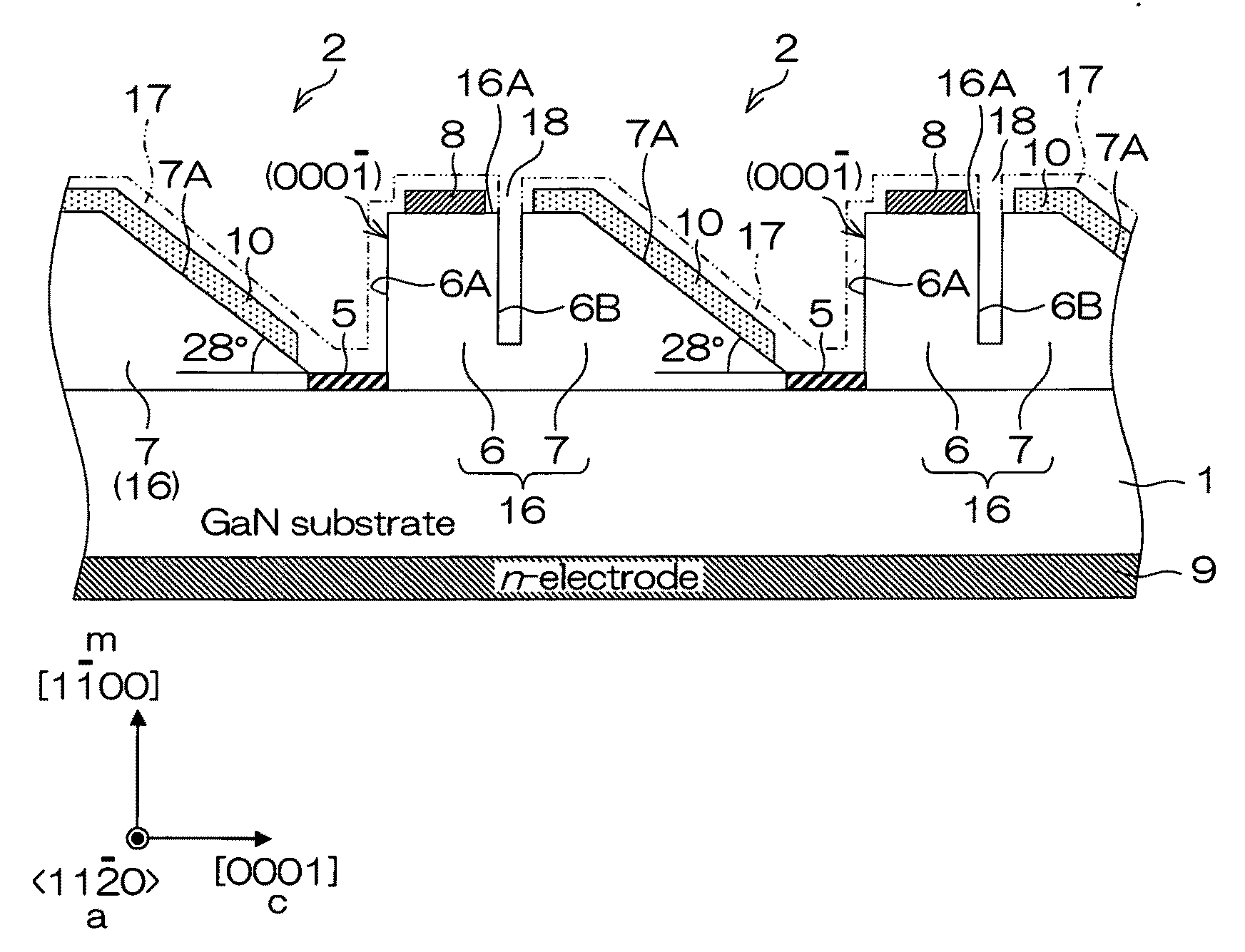
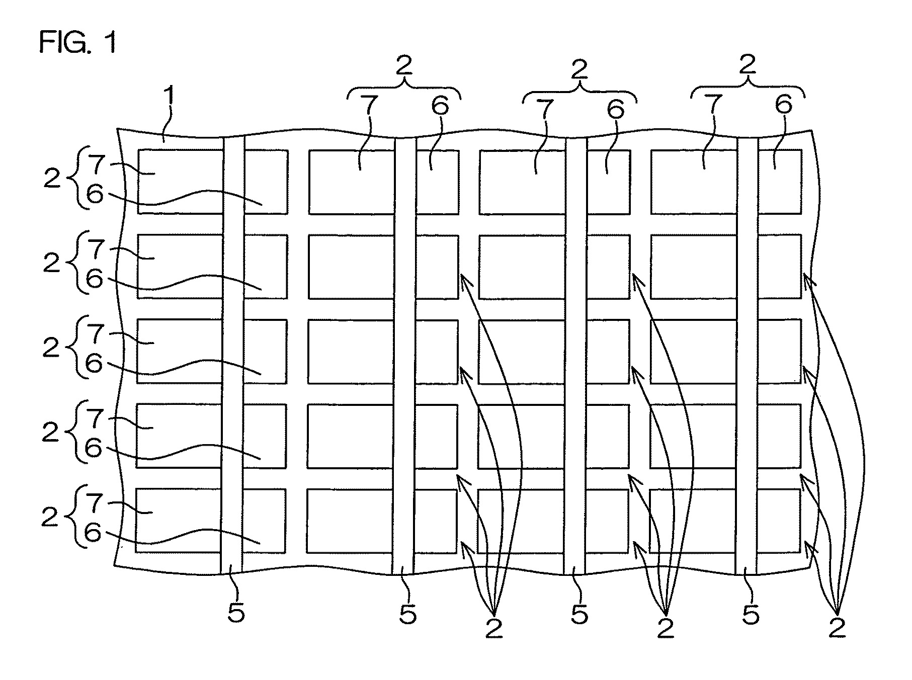
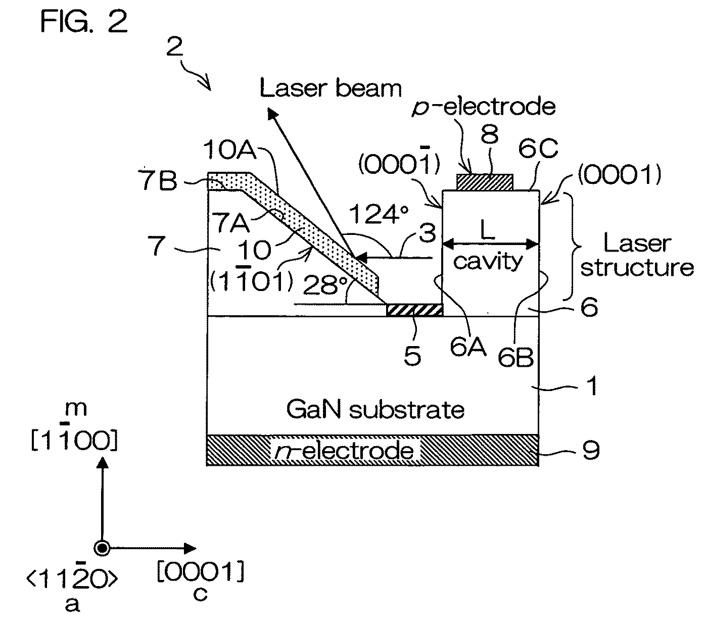
[0017]A semiconductor light emitting device according to an embodiment of the present invention includes an optical cavity (the so-called horizontal cavity having a cavity direction parallel to a major growth surface) made of a group III nitride semiconductor having a major growth surface defined by a nonpolar plane and including a pair of cavity end faces parallel to c-planes, and a reflecting portion made of a group III nitride semiconductor having a major growth surface defined by a nonpolar plane and having a reflective facet opposed to one of the pair of cavity end faces and inclined with respect to the normal of the major growth surface.

[0018]According to this structure, the optical cavity emits light in a direction parallel to the major growth surface of the group III nitride semiconductor, and the light is applied to the reflective facet. The reflective facet is inclined with respect to the normal of the major growth surface, whereby the light reflected by the reflecting por...


PUM


Abstract

This semiconductor light emitting device includes an optical cavity made of a group III nitride semiconductor having a major growth surface defined by a nonpolar plane and including a pair of cavity end faces parallel to c-planes, and a reflecting portion made of a group III nitride semiconductor having a major growth surface defined by a nonpolar plane and having a reflective facet opposed to one of the pair of cavity end faces and inclined with respect to a normal of the major growth surface. The optical cavity and the reflecting portion may be crystal-grown from the major surface of the substrate. The substrate is preferably a group III nitride semiconductor substrate having a major surface defined by a nonpolar plane.

Description

BACKGROUND OF THE INVENTION[0001]1. Field of the Invention[0002]The present invention relates to a semiconductor light emitting device employing group III nitride semiconductors and a method of manufacturing the same. Group III nitride semiconductors are group III-V semiconductors employing nitrogen as a group V element, and typical examples thereof include aluminum nitride (AlN), gallium nitride (GaN) and indium nitride (InN), which can be generally expressed as AlxInyGa1-x-yN (0≦x≦1, 0≦y≦1 and 0≦x+y≦1).[0003]2. Description of Related Art[0004]A semiconductor laser perpendicularly emitting light from a major surface of a semiconductor substrate is referred to as a surface emitting laser. In a general surface emitting laser, a cavity is formed by arranging reflecting mirrors on upper part and lower part of a semiconductor thin film, with a cavity direction parallel to a normal direction of the major surface of the semiconductor substrate.[0005]In the surface emitting laser having th...

Claims


Application Information

Patent Timeline
IPC IPC(8): H01L33/00H01S5/026H01S5/185H01S5/22
CPCB82Y20/00H01S5/026H01S5/34333H01S5/2201H01S5/3202H01S5/18H01S5/0071H01S5/32025H01S5/0203H01S5/185
Inventor KUBOTA, MASASHIOKAMOTO, KUNIYOSHI
Owner ROHM CO LTD
Why Eureka
Try Eureka