Method and device for avoiding image sticking

a liquid crystal display and image sticking technology, applied in the field of circuits and liquid crystal display panel parts, can solve problems such as image sticking generation, and achieve the effect of avoiding image sticking generation and avoiding image sticking

Active Publication Date: 2009-03-26
BEIJING BOE OPTOELECTRONCIS TECH CO LTD +1
View PDF2 Cites 10 Cited by
  • Summary
  • Abstract
  • Description
  • Claims
  • Application Information

AI Technical Summary

Benefits of technology

[0007]An object of the present invention provides a method and a device for avoiding image sticking, which are used to resolve the image sticking problem in the prior art in order to realize dynamically adjusting common electrode voltage to be consistent with an ideal value thereby avoiding image sticking generation.

Problems solved by technology

Therefore, if only one fixed common electrode voltage is inputted or the real common electrode voltage is adjusted according to a specific coupling voltage generated at a time, there is a difference between the real common electrode voltage and the ideal common electrode voltage and the influence of the coupling voltage can not be removed, such that the image sticking is generated.

Method used


Image

  • Method and device for avoiding image sticking
  • Method and device for avoiding image sticking
  • Method and device for avoiding image sticking

Examples


first embodiment

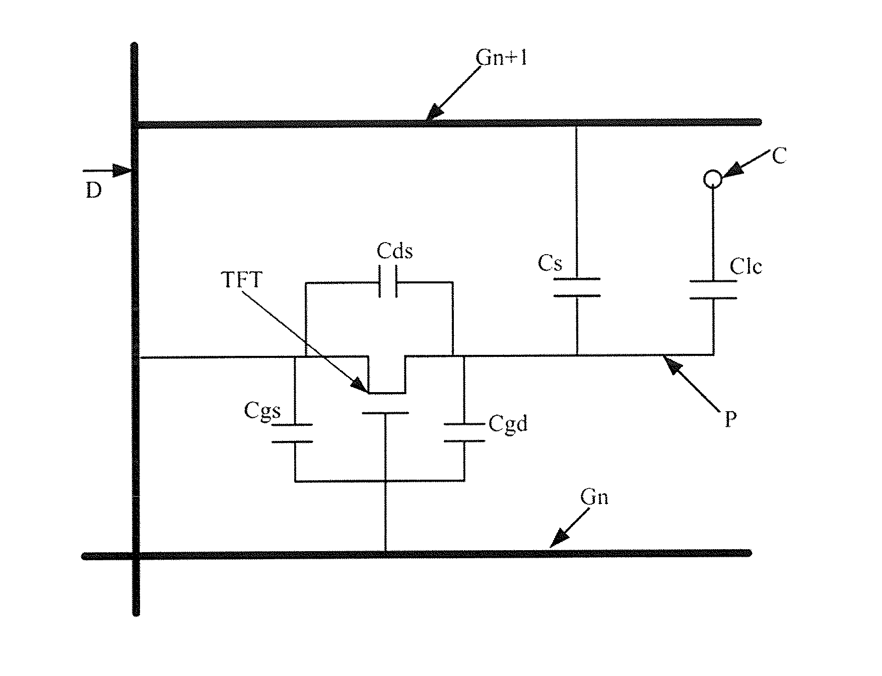
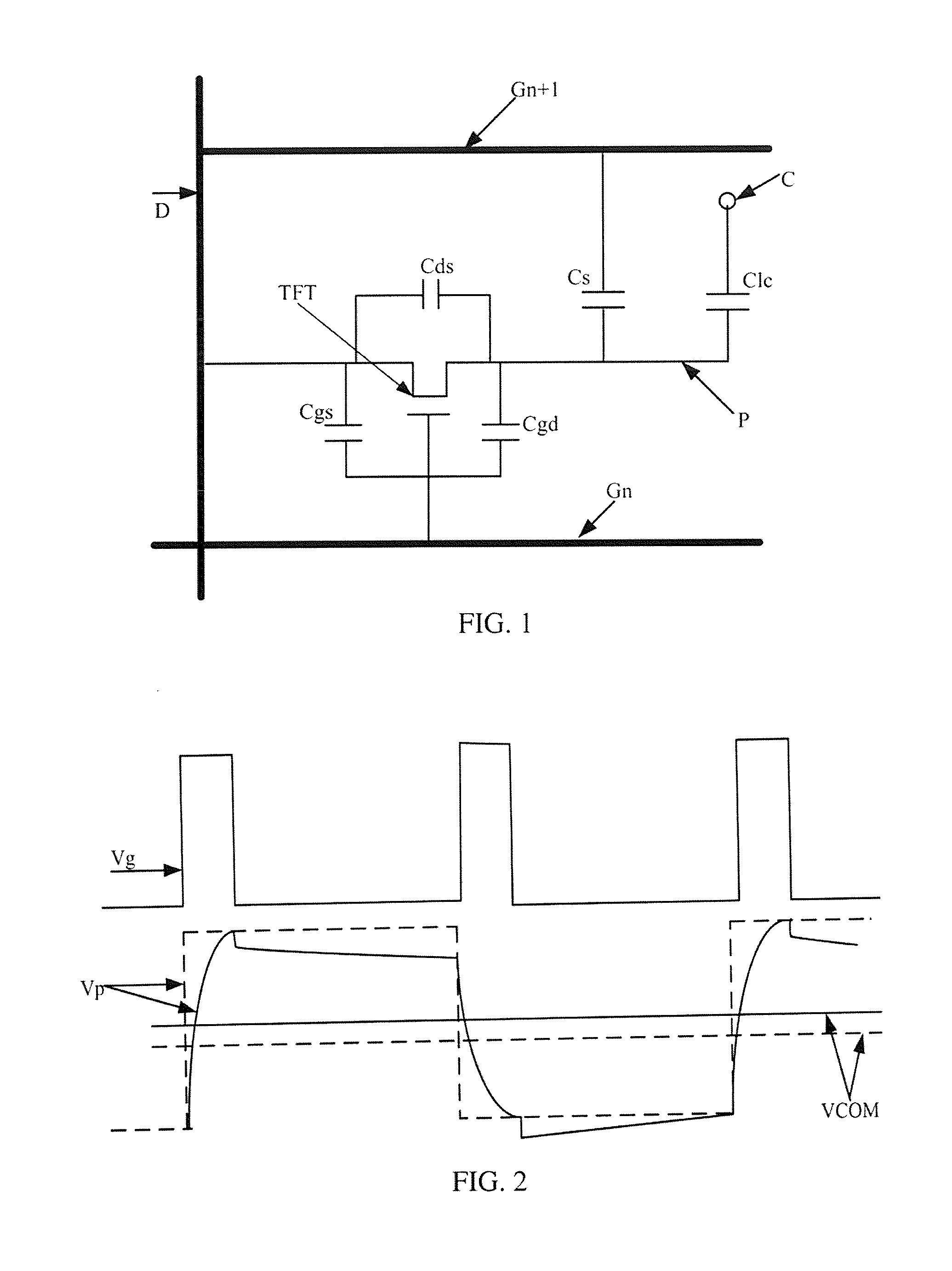
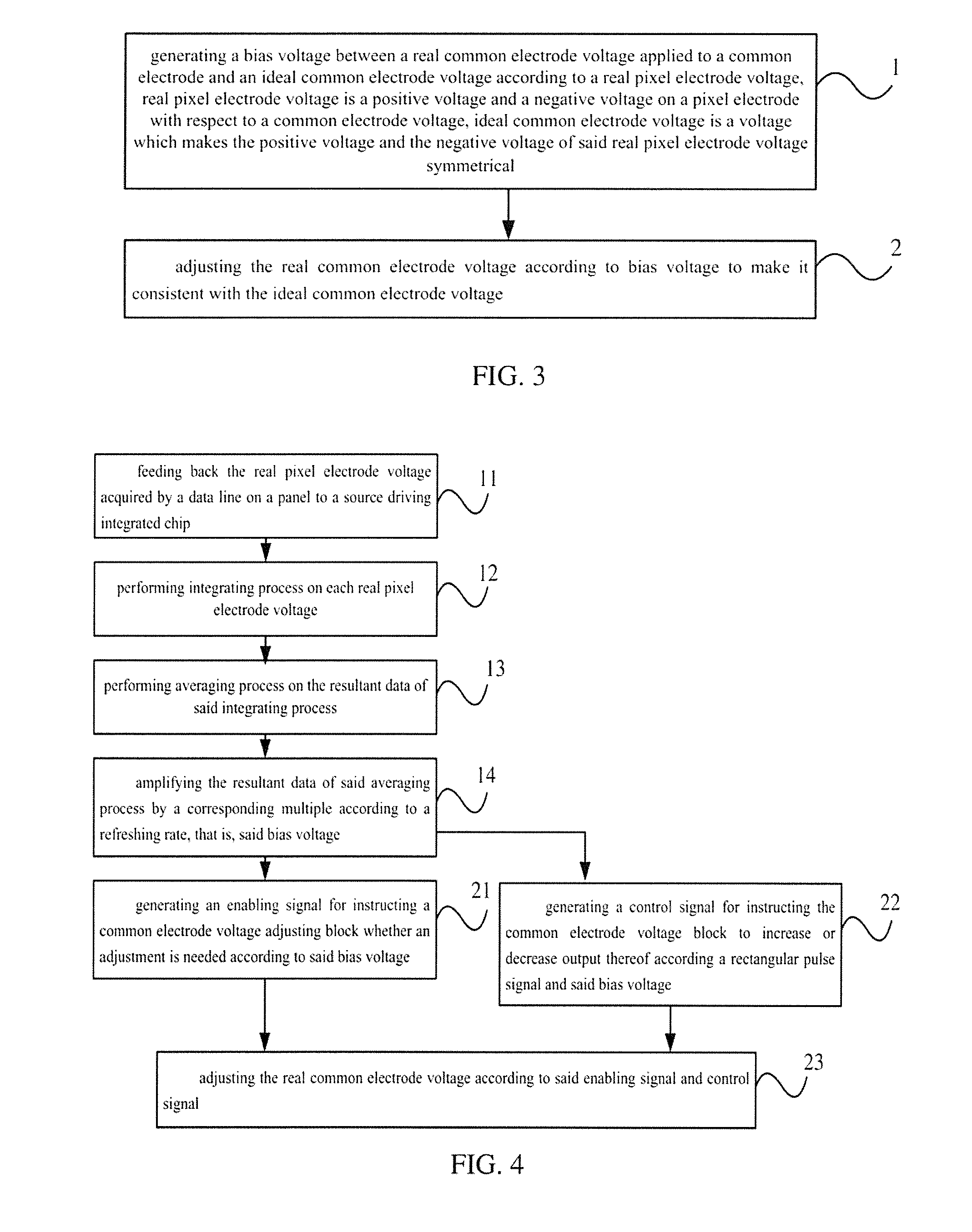
[0029]As shown in FIG. 3 which is a flowchart of the method for avoiding image sticking according to the present invention. A method for avoiding image sticking comprises:

[0030]step 1: generating a bias voltage between a real common electrode voltage applied to a common electrode and an ideal common electrode voltage according to a real pixel electrode voltage, wherein said real pixel electrode voltage is a positive voltage and a negative voltage on a pixel electrode with respect to a common electrode voltage, said ideal common electrode voltage is a voltage which makes the positive voltage and the negative voltage of said real pixel electrode voltage symmetrical;

[0031]step 2: adjusting the real common electrode voltage according to said bias voltage to make it consistent with the ideal common electrode voltage.

[0032]This embodiment makes the real common electrode voltage consistent with the ideal common electrode voltage by comparing the real common electrode voltage consistent wit...

second embodiment

[0033]As shown in FIG. 4 which is a flowchart of the method for avoiding image sticking according to the present invention. A method for avoiding image sticking comprises:

[0034]step 11: feeding the real pixel electrode voltage acquired by a data line on a panel back to a source driving integrated chip in order to complete data acquisition, to provide input data for computing the bias voltage, where number of data lines is determined based on real situation, and the number is larger, an average number is finer with possible aperture ratio drop;

[0035]step 12: performing integrating process on each said real pixel electrode voltage; according to integrator principle, the resultant value of integration of each integrator is A times of bias voltage between the real common electrode voltage of pixel corresponding to that integrator and the ideal common electrode voltage, A=1 / refreshing rate (a specific value for times A is associated with a refreshing rate, a generic refreshing rate is be...


PUM


Abstract

The present invention directs to a method an device for avoiding image sticking, the method for avoiding image sticking is to adjust a real common electrode voltage by difference between the real common electrode voltage and an ideal common electrode voltage, said difference is obtained by acquiring a real pixel electrode voltage on a panel; the device comprises a difference generation block for generating the difference between the real common electrode and the ideal common electrode voltage and an adjusting block for adjusting the real common electrode voltage, said adjusting block comprises an enabling block for generating a common electrode voltage adjustor enabling signal, a control block for generating a common electrode voltage adjustor control signal, and a common electrode voltage adjustor for adjusting the real common electrode voltage. With the method and device of the present invention, the coupling voltage's influence on a pixel electrode can be eliminated, and image sticking can be alleviated or avoided, and no impact on flicker is generated.

Description

TECHNICAL FIELD [0001]The present invention directs to a circuit and a panel portion of liquid crystal display, in particular, to a method and a device for avoiding image sticking, which are capable of dynamically adjusting a real common electrode voltage.BACKGROUND ART [0002]A thin film transistor active matrix liquid crystal display (TFT-LCD) is a advanced product in the current liquid crystal display (LCD) market. With development of thin film transistor process, the TFT-LCD has become a popular product in the current LCD market. FIG. 1 is an equivalent circuit diagram of sub pixel of an existing panel, which comprises gate line Gn, data line D, TFT, parasitic capacitor Cgd between gate and drain of TFT, parasitic capacitor Cgs between gate and source, parasitic capacitor Cds between drain and source, two terminals of the liquid crystal capacitor C1c are respectively connected to a common electrode C and a pixel electrode P, and one terminal of the storage capacitor Cs is connect...

Claims


Application Information

Patent Timeline
Patent Type & Authority Applications(United States)
IPC IPC(8): G06F3/038
CPCG09G3/3611G09G3/3648G09G2320/0252G09G3/3696G09G3/3655G09G3/36G09G3/20G02F1/133
Inventor DOU, FANG
Owner BEIJING BOE OPTOELECTRONCIS TECH CO LTD
Why Eureka
Try Eureka