Wafer-Shaped Measuring Apparatus and Method for Manufacturing the Same

a measuring apparatus and wafer-shaped technology, applied in the direction of instruments, heat measurement, thermometer details, etc., can solve the problems of affecting treatment, difficulty in accurately measuring the temperature of each measuring point of the wafer, etc., and achieve the effect of favorable measuring performance and high thermal conductivity

Inactive Publication Date: 2009-04-02
TOKYO ELECTRON LTD
View PDF6 Cites 9 Cited by
  • Summary
  • Abstract
  • Description
  • Claims
  • Application Information

AI Technical Summary

Benefits of technology

[0005]For this reason, a temperature measuring apparatus with favorable temperature measuring performance capable of favorably conducting heat from the wafer to the temperature sensor and a method for manufacturing the same has been desired.
[0014]According to the present invention, by contacting the sensor on the wafer and wafer using a high thermal conductivity material, a wafer-shaped measuring apparatus with favorable measuring performance and a method for manufacturing the same can be provided.

Problems solved by technology

However, when this contact layer has factors that heat is not favorably conducted from the wafer to the temperature, such as a low thermal conductivity or unevenness in the thickness of this contact layer, a problem of difficulty in accurately measuring the temperature for each measuring point of the wafer may occur.
As a result, the temperature distribution of the hot plate or the like can not be accurately measured and resulting in a problem of negatively affecting the treatments.

Method used


Image

  • Wafer-Shaped Measuring Apparatus and Method for Manufacturing the Same
  • Wafer-Shaped Measuring Apparatus and Method for Manufacturing the Same
  • Wafer-Shaped Measuring Apparatus and Method for Manufacturing the Same

Examples


Embodiment Construction

[0036]A temperature measuring apparatus and a manufacturing method for the same according to embodiments of the present invention will be described referring to drawings.

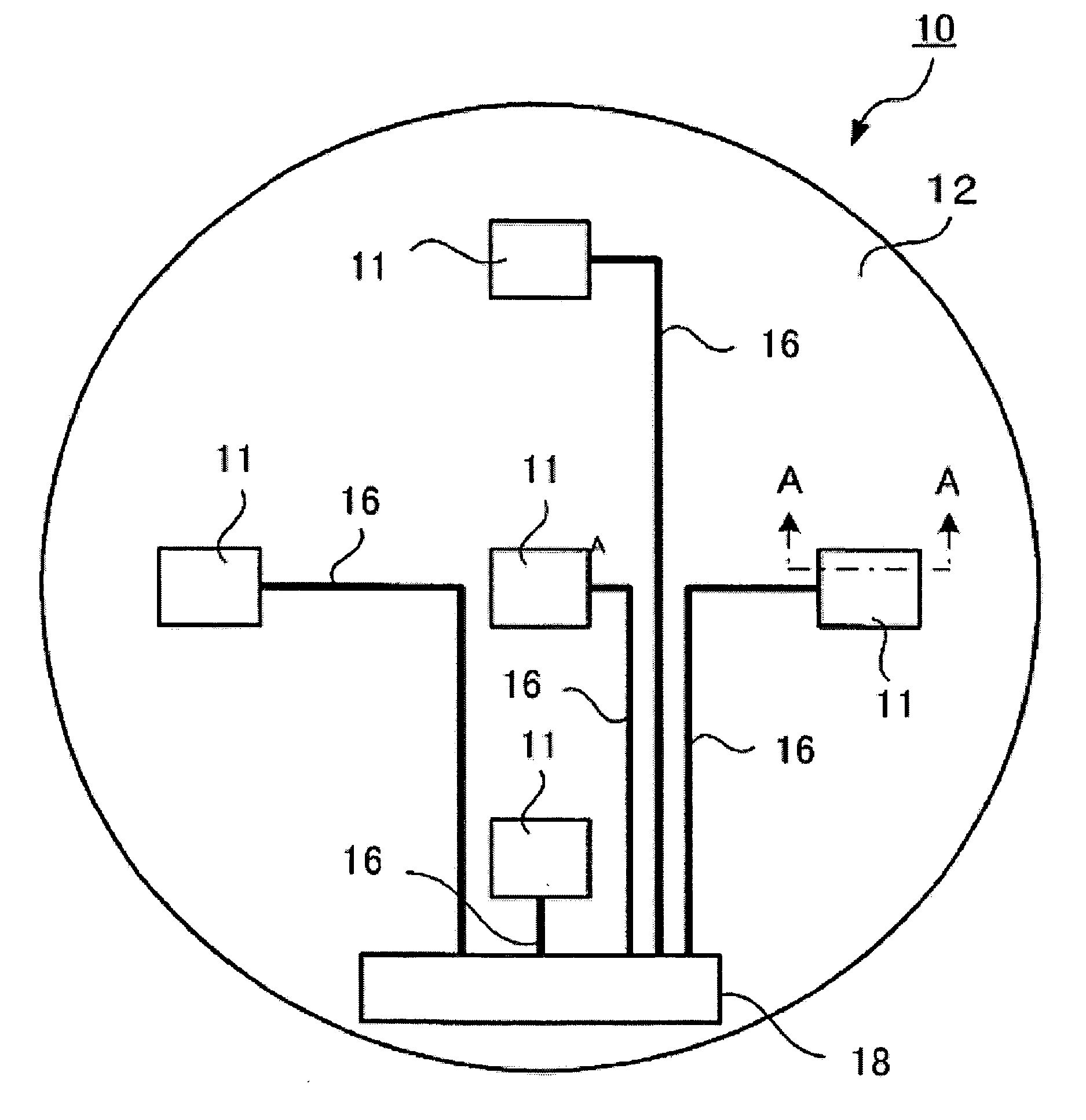
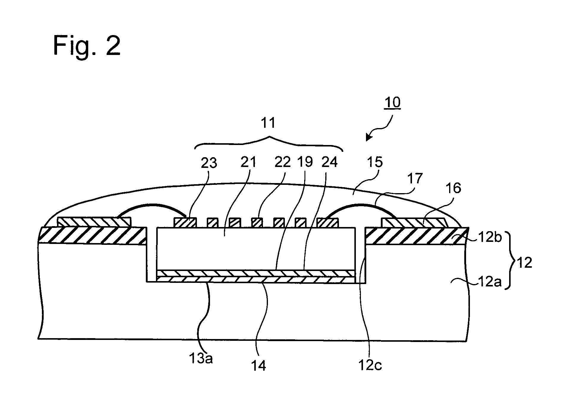
[0037]FIGS. 1 to 4 illustrate a temperature measuring apparatus 10 pertaining to an embodiment of the present invention. FIG. 1 is a plane view of the temperature measuring apparatus 10. FIG. 2 is an A-A line cross section diagram of the temperature measuring apparatus 10 in FIG. 1. FIG. 3(a) is a plane view of a temperature sensor 11, which configures the temperature measuring apparatus 10. FIG. 3(b) is a B-B line cross section diagram of FIG. 3(a). FIG. 4(a) is a plane view of a semiconductor wafer 12 in an area where the temperature sensor 11 is provided. FIG. 4(b) is a C-C line cross section of FIG. 4(a).

[0038]As shown in FIGS. 1 to 4, the temperature measuring apparatus pertaining to the embodiment includes the temperature sensor 11, the semiconductor wafer 12, a first contact layer 14, a protection film 15, a ...


PUM


Abstract

The present invention provides a temperature measuring apparatus with favorable temperature measuring performance and a method of manufacturing the same. A temperature measuring apparatus (10) provided with a temperature sensor (11) arranged on a bottom surface of a depressed section (12c) of a semiconductor wafer (12). The semiconductor wafer (12) and temperature sensor (11) are contacted together through a first contact layer (14) and second contact layer (24). The first and second contact layers (14) and (24) are formed from the same material, concretely a metal with high heat conductivity, and formed to provide virtually even thickness in surface direction. By such first and second contact layers (14) and (24), heat is conducted from the semiconductor wafer (12) to the temperature sensor (11) favorably. Therefore, the temperature measuring apparatus (10) has favorable temperature measuring performance.

Description

TECHNICAL FIELD[0001]The present invention relates to a wafer-shaped measuring apparatus for measuring conditions of wafer processes, and method for manufacturing the same, particularly relates to a temperature measuring apparatus for measuring semiconductor wafers and a method for manufacturing the same.BACKGROUND ART[0002]Conventionally, in a manufacturing process of semiconductor devices, processes for thermally treating a semiconductor wafer (hereinafter referred as a wafer), such as a heat treatment for drying after applying resist solution, a heat treatment after exposure (post exposure baking), and CVD treatment when forming a predetermined thin film on a wafer surface, have been performed. In order to improve yield, the temperature within the wafer surface needs to be as even as possible when performing these thermal treatments.DISCLOSURE OF INVENTIONProblems to be Solved by the Present Invention[0003]For example, in a hot plate unit, in which baking processes, such as post ...

Claims


Application Information

Patent Timeline
Patent Type & Authority Applications(United States)
IPC IPC(8): H01L23/58H01L21/00
CPCG01K1/16H01L21/67248G01K7/01H01L2224/83192H01L2924/181H01L2224/48091H01L2224/73265H01L2224/92247H01L2924/00014H01L2924/00012
Inventor MATSUDA, KENJIMINAMI, TOMOHIDEYAMANISHI, YOSHIKIHARADA, MUNEO
Owner TOKYO ELECTRON LTD
Why Eureka
Try Eureka