Illumination optical system, exposure apparatus, and device manufacturing method

a technology of exposure apparatus and optical system, which is applied in the direction of photomechanical treatment, printing, instruments, etc., can solve the problems of difficult control of impurities contained, degradation of chip yield, and decrease of interference fringe contrast in resist, etc., and achieve high purity of polarization

Inactive Publication Date: 2009-04-02
CANON KK
View PDF14 Cites 8 Cited by
  • Summary
  • Abstract
  • Description
  • Claims
  • Application Information

AI Technical Summary

Benefits of technology

[0045]According to the present invention, it is possible to provide a technique advantageous to obtaining target polarization states with, e.g., high purity of polarization.

Problems solved by technology

Unfortunately, the recent study has revealed that along with an increase in NA, p-polarized light (a light component whose electric field vector lies on a plane including the light component and the normal to the substrate when it strikes the substrate) decreases the contrast of interference fringes in the resist.
In this case, the image contrast decreases and therefore an ED window reduces, resulting in degradation in the yield of a chip.
A crystal of quartz crystal having a diameter larger than that value takes much time for crystal growth, and it is difficult to control impurities contained in it.
For these reasons, such a crystal is very expensive and is therefore hard to supply stably.
However, at the position at which the incident angle is small, the light beam diameter is large, so a required size of the waveplate is large.
The size of the waveplate is subject to the limitations on the manufacture of the birefringent glass material, as described above.
This makes it impossible to obtain a good purity of polarization.

Method used


Image

  • Illumination optical system, exposure apparatus, and device manufacturing method
  • Illumination optical system, exposure apparatus, and device manufacturing method
  • Illumination optical system, exposure apparatus, and device manufacturing method

Examples


Embodiment Construction

[0060]A preferred embodiment of the present invention will be described below with reference to the accompanying drawings.

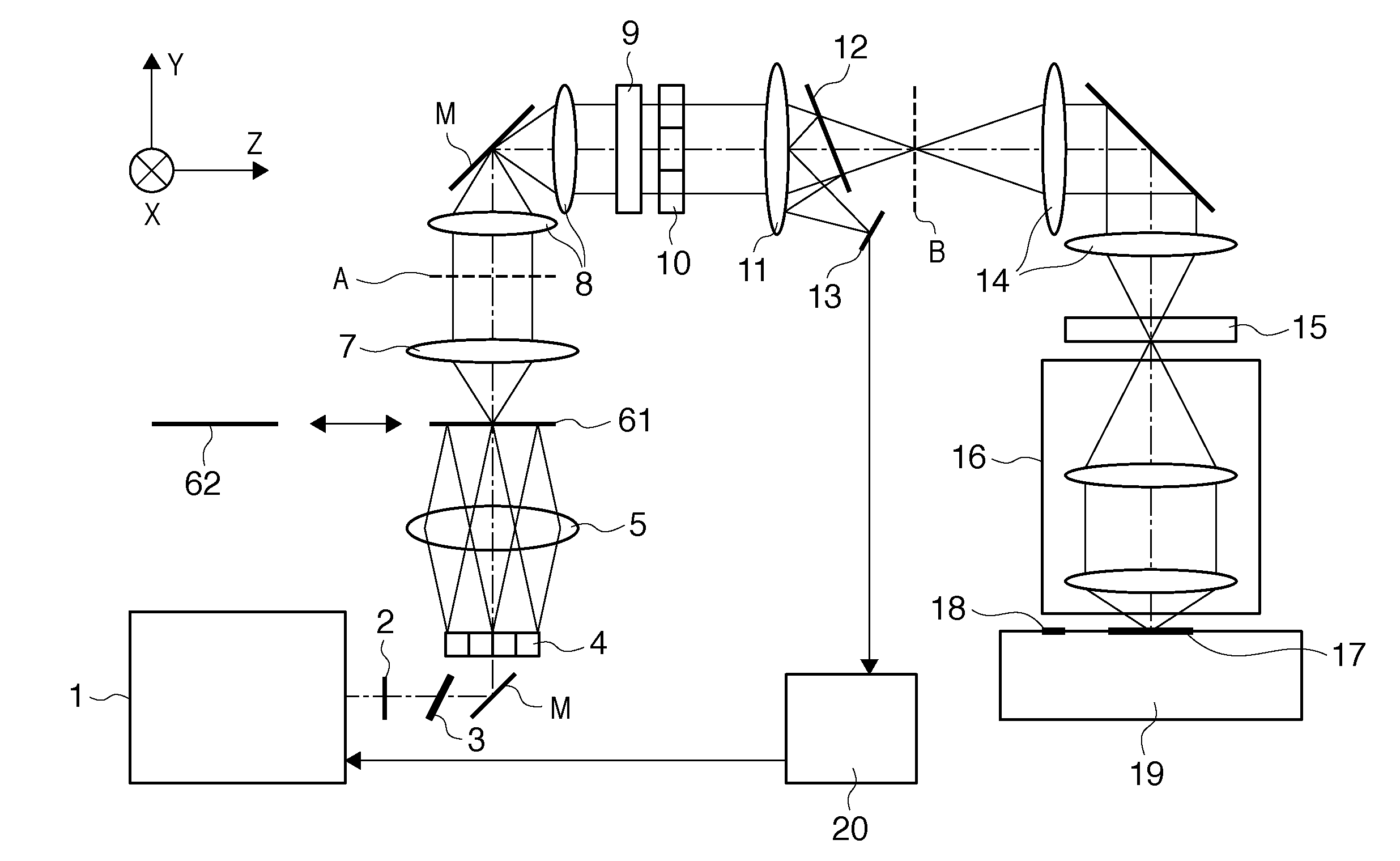
[0061]FIG. 13 is a view showing the schematic arrangement of an exposure apparatus according to a preferred embodiment of the present invention. The same reference numerals as in FIG. 5 denote the same constituent elements in FIG. 13, and a description thereof will not be repeated. The exposure apparatus shown in FIG. 13 has an arrangement in which the waveplate 2 and polarization control unit 9 in the illumination optical system of the exposure apparatus shown in FIG. 5 are replaced by a first polarization control unit 2′ and second polarization control unit 9′, respectively.

[0062]The exposure apparatus according to the preferred embodiment of the present invention can comprise an illumination optical system IL for illuminating an original (also called a reticle or mask) 15 or its part as the target illumination region with light provided by a light source 1, an...


PUM


Abstract

An illumination optical system comprises a first polarization control unit which is located between a light source and a pupil of an illumination optical system, and a second polarization control unit which is located between the first polarization control unit and the pupil, wherein a region on the pupil includes a plurality of partial regions which are classified into a first group including a partial region having a largest area, and a second group including a partial region different from the partial region having the largest area, and the second polarization control unit controls a polarization state in the partial region which belongs to only the second group.

Description

BACKGROUND OF THE INVENTION[0001]1. Field of the Invention[0002]The present invention relates to an illumination optical system, an exposure apparatus, and a device manufacturing method.[0003]2. Description of the Related Art[0004]Devices such as a semiconductor device can be manufactured by a lithography process. A projection exposure apparatus is used in the lithography process. The lithography process includes a process of projecting a circuit pattern onto a substrate (e.g., a silicon substrate or glass substrate) coated with a photosensitive material, thereby transferring the circuit pattern onto the photosensitive material.[0005]Along with the recent advance of the micropatterning of semiconductor devices, a pattern having a line width of 0.15 μm or less is transferred onto a substrate. The advance of the micropatterning of semiconductor devices improves the packing density, which makes it possible to manufacture low-power, high-performance semiconductor devices. Under the circ...

Claims


Application Information

Patent Timeline
Patent Type & Authority Applications(United States)
IPC IPC(8): G03B27/72
CPCG03F7/70566G03F7/70091
Inventor MORI, KENICHIRO
Owner CANON KK
Why Eureka
Try Eureka