
Retention improvement in dual-gate memory

a dual-gate memory and charge retention technology, applied in the direction of basic electric elements, electrical equipment, semiconductor devices, etc., can solve the problems of charge retention, difficulty in maintaining clear distinction between erased and programmed threshold voltages, and the lateral charge motion within the nitride-containing charge-trapping medium is a problem, so as to achieve the effect of minimizing the lateral charge motion problem

Inactive Publication Date: 2009-04-02
SCHILTRON
View PDF4 Cites 3 Cited by
  • Summary
  • Abstract
  • Description
  • Claims
  • Application Information

AI Technical Summary

Benefits of technology

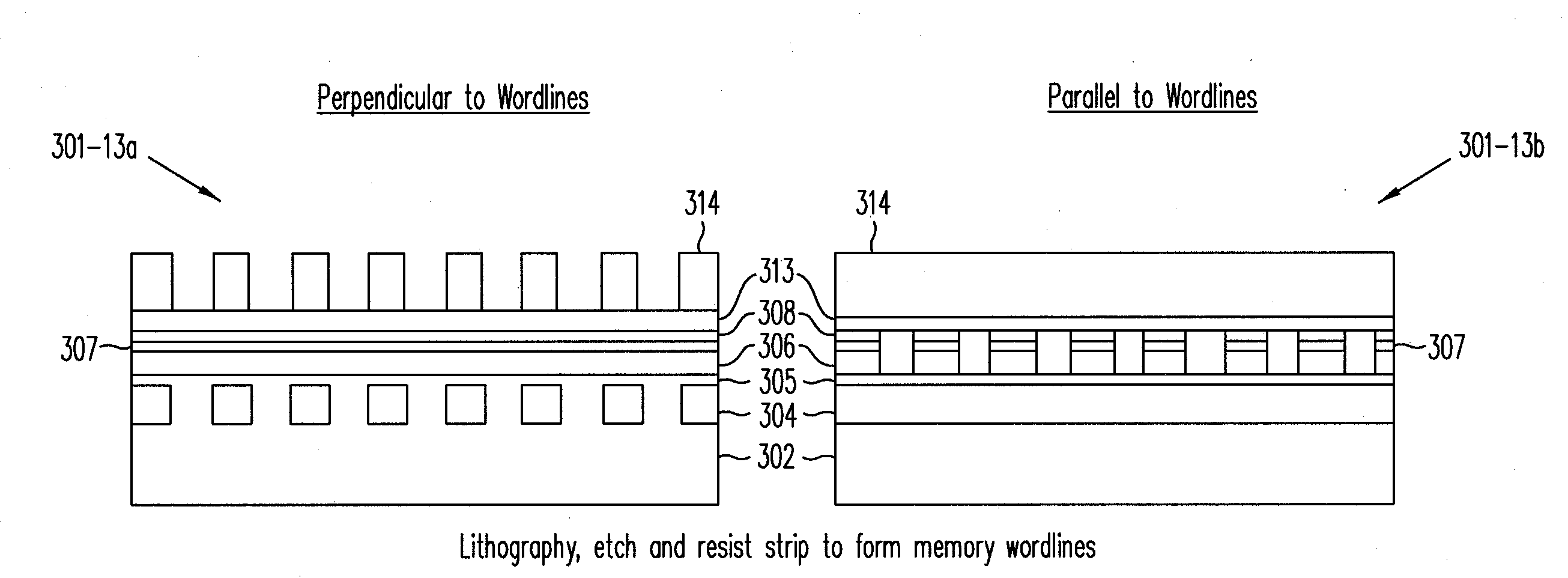
[0008]The present patent application describes a method for preventing lateral charge motion and addresses data retention issues in dual-gate non-volatile memory cells. According to the present invention, a method limits the lateral extent of the charge-trapping medium (e.g., silicon nitride) in a dual-gate non-volatile memory cell. In this way, retention problems associated with lateral motion of charge can be minimized.

Problems solved by technology

In series-connected transistors that act as nonvolatile memory cells with nitride charge storage (e.g., in Jung's NAND configuration), lateral charge motion within the nitride-containing charge-trapping medium is a problem.
Lateral charge motion within the charge-trapping medium results in both a charge retention problem and a difficulty in maintaining clear distinction between the erased and programmed threshold voltages.

Method used


Image

  • Retention improvement in dual-gate memory
  • Retention improvement in dual-gate memory
  • Retention improvement in dual-gate memory

Examples


Embodiment Construction

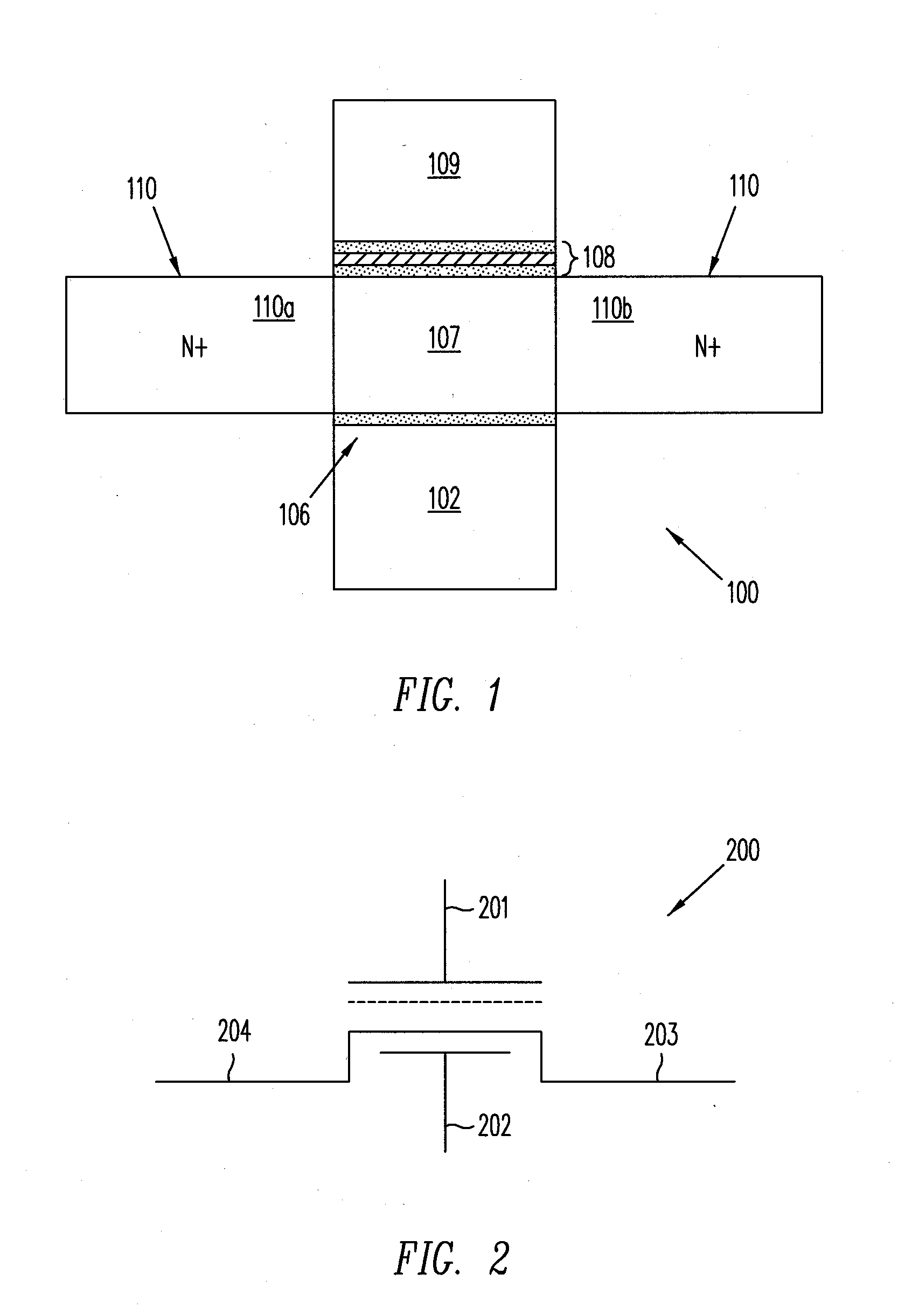
[0013]FIG. 1 is a schematic cross-section of dual-gate memory cell 100 formed by a memory device and a non-memory device (also, referred to as an “access device”). As shown in FIG. 1, the access device includes gate dielectric 106 and gate electrode 102 and the memory device includes gate dielectric stack 108 and gate electrode 109. Gate dielectric stack 108 includes a charge-trapping layer that stores charge in a non-volatile fashion. The memory and access devices share source and drain regions 110 and active region 107., Although shown having the memory device formed above the access device, these device may be formed in the reverse order—i.e., with the memory device formed underneath the access device. FIG. 2 is a graphical representation 200 of a dual-gate device, indicating gate electrode 201 of the memory device, and gate electrode 202 of the access device, with source and drain connections 203 and 204.

[0014]The advantages of dual-gate non-volatile memory cells are discussed, ...


PUM


Abstract

A manufacturing process improves retention capabilties of dual-gate non-volatile memory cells by limiting the effects of lateral charge movement. The process limits lateral extents of the charge storage medium that is an integral part of the memory device within the dual-gate device.

Description

CROSS REFERENCE TO RELATED APPLICATIONS[0001]The present application relates to and claims priority of U.S. provisional patent application (“Provisional Application”), entitled “Retention Improvement in Dual-Gate Memory,” Ser. No. 60 / 977,007, filed on Oct. 2, 2007. The disclosure of the Provisional Application is hereby incorporated by reference in its entirety.BACKGROUND OF THE INVENTION[0002]1. Field of the Invention[0003]The present invention relates to methods for optimizing charge retention in nonvolatile memories consisting of strings of serially connected dual-gate memory cells.[0004]2. Discussion of the Related Art[0005]Thin-film transistors having silicon nitride as the charge storage medium may be used as building blocks for three-dimensionally integrated non-volatile memories. In that regard, the article “3D-TFT SONOS Memory Cell for Ultra-High Density File Storage Applications” (“Walker”), by Walker et al., published in the Symposium on VLSI Technology, Kyoto 2003, repor...

Claims


Application Information

Patent Timeline
Patent Type & Authority Applications(United States)
IPC IPC(8): H01L21/3205
CPCH01L27/12H01L27/11568H10B43/30
Inventor WALKER, ANDREW J.
Owner SCHILTRON
Learn More