
Protecting device for electronic circuit and manufacturing method thereof

a protection device and electronic circuit technology, applied in the direction of spark plugs, discharge tubes/lamp details, coatings, etc., can solve the problems of not reaching the necessary scale, extending to the loss of the whole electronic product, and severe damage to the components of electronic equipmen

Inactive Publication Date: 2009-04-09
INPAQ TECH
View PDF3 Cites 16 Cited by
  • Summary
  • Abstract
  • Description
  • Claims
  • Application Information

AI Technical Summary

Benefits of technology

[0015]Accordingly, the present invention has been made to solve the above-mentioned problems occurring in the prior art, and an object of the present invention is to provide a protecting device for electronic circuit and manufacturing method thereof such that the electronic circuit can be protected from being damaged due to a surge voltage.
[0016]In order to accomplish the object, there is provided a method of manufacturing a protecting device for electronic circuit to form a stacked structure on a substrate, and to form a dielectric layer thereof using the printing process, and cutting a gap thereof. By utilizing materials of different properties for the dielectric layer, a protecting device can be produced which is able to protect an electronic circuit involving various kinds of resistor, capacitor, and inductor. While the gap may become a protecting element for ESD. by filling a piezoelectrically sensitive material or various gases etc. therein, and then to serve as an element having function of preventing the electronic apparatus from damage by ESD.
[0017]According to the protecting device for electronic circuit and manufacturing method of present invention, a multi-layered structure is formed which includes a dielectric layer and severed electrode layers overlapping one another in the inner circumference of the substrate. After making up a whole structure, a transverse gap with an appropriate depth is formed by cutting process which causes two superposed electrode layers to split into two parts facing to each other with respect to the transverse gap, and also split into upper and lower parts with respect to the dielectric layer. With this structure, the gap can serve as a protecting element for ESD by filling different kinds of materials and with the aid of the dielectric layer of appropriate thickness thereby the whole structure can be used to perform protection for various electronic circuits.
[0019]According to the protecting device for electronic circuit and manufacturing method of present invention, the distance between the upper and the lower electrode layers is determined by the thickness of the dielectric layer formed by printing process. Accordingly, the high difference between the upper electrode layer and the lower electrode layer can be controlled as small as possible so as to prevent an unappropriate breakdown voltage caused by an improper gap width.
[0020]According to the protecting device for electronic circuit and manufacturing method thereof, the structure of the protecting device is made very simple while having versatile performance, and can be made up with a low production cost.

Problems solved by technology

In the circuit of electronic communication, an abnormal voltage caused by the electro-static discharge (ESD) may cause a severe damage to the components of the electronic equipment such as a substrate and which further extends to the loss of the whole electronic product.
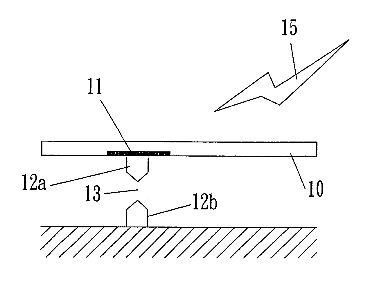
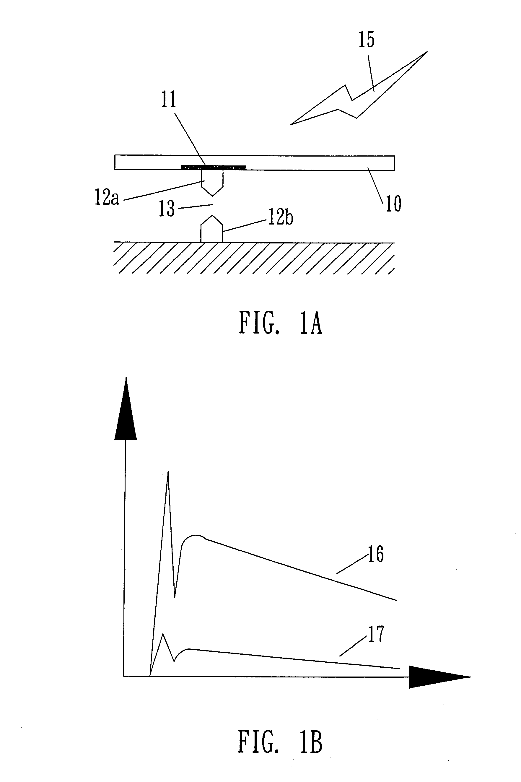
(1) The gap 13 which is formed by mechanical cutting can not achieve the necessary scale sufficient to protect the surge of ESD.
(2) As the width of the gap 13 can not reach the required scale, the break down voltage will become high and then is not possible to protect the electronic circuit and device.
For these defects noticeable on the prior art, an improvement is seriously required.

Method used


Image

  • Protecting device for electronic circuit and manufacturing method thereof
  • Protecting device for electronic circuit and manufacturing method thereof
  • Protecting device for electronic circuit and manufacturing method thereof

Examples


Embodiment Construction

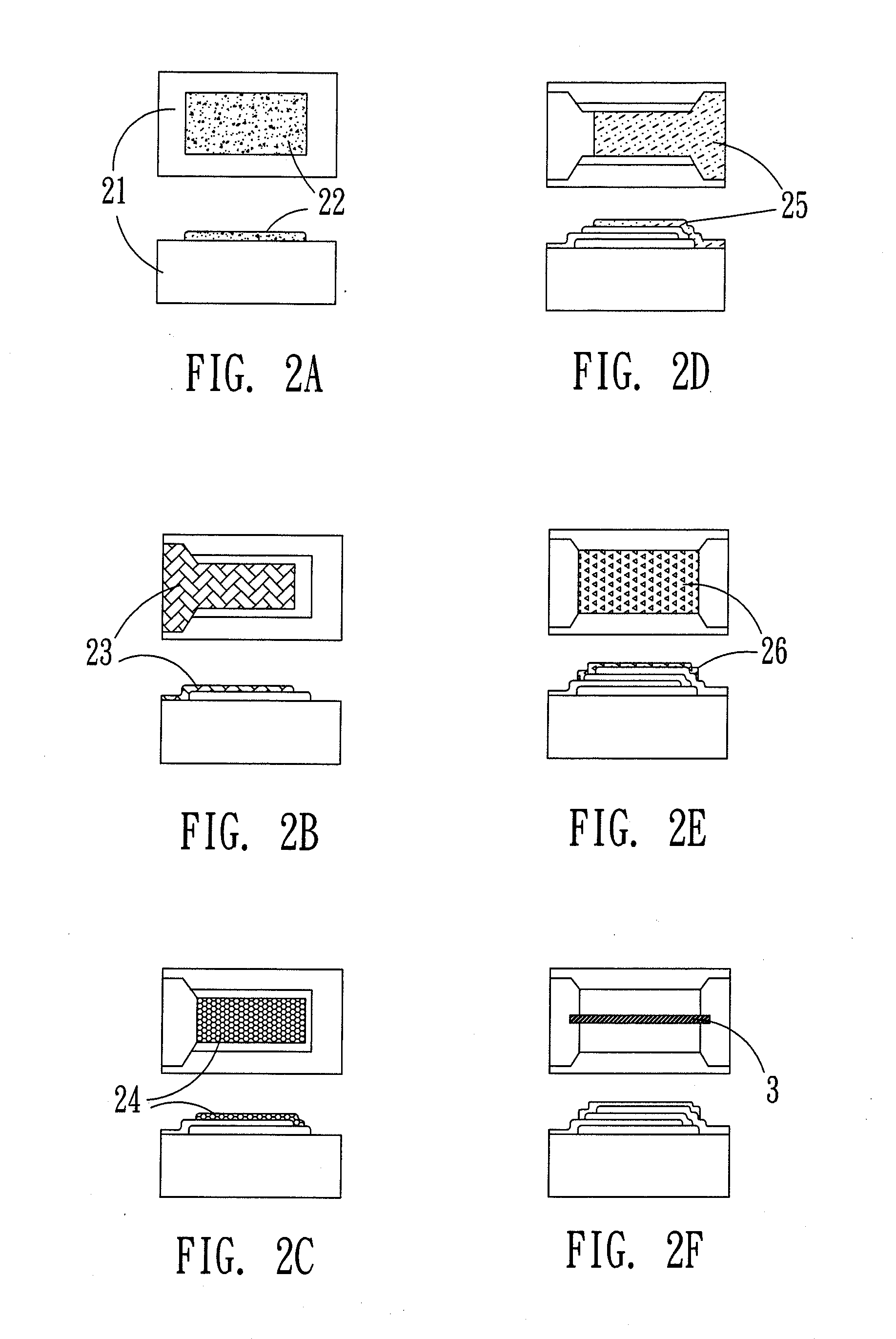
[0029]As shown in FIG. 2A through 2F, the manufacturing method of the protecting device for electronic circuit of present invention includes the following steps of:

[0030]1. Forming a glass foundation 22 on the surface of a ceramic substrate 21, wherein the glass foundation 22 is positioned on the central part of the ceramic substrate 21 to avoid contacting it edges with that of the ceramic substrate 21 (please refer to FIG. 2A);

[0031]2. Forming a first electrode layer 23 to cover the glass foundation 22, one side of the first electrode layer 23 is connected with a first side of the ceramic substrate 21, while the other side thereof is partially covering the upper surface of the glass foundation 22 (please refer to FIG. 2B);

[0032]3. Forming a dielectric layer 24 having the area approximately equal to that of the glass foundation 22 to cover the first electrode layer 23 at a position right on the glass foundation 22, one side of the dielectric layer 24 is connected to one side of the ...


PUM


Abstract

Disclosed is a protecting device for electronic circuit and the manufacturing method thereof. The device is a multi-layered structure which includes a dielectric layer and several electrode layers overlapping in the inner circumference of the substrate. After making up a whole structure, a transverse gap with an appropriate depth is formed by cutting process causing two superposed electrode layers to split into two parts facing to each other with respect to the transverse gap and also split into upper and lower parts with respect to the dielectric layer. With this structure, the gap can serve as a protecting element for electrostatic discharge (ESD) or other elements by filling different materials and with the aid of the dielectric layer of appropriate thickness thereby the whole structure can be used to perform surge protection for various electronic circuits.

Description

BACKGROUND OF THE INVENTION[0001]1. Field of the Invention[0002]The present invention relates to a protecting device for electronic circuit and manufacturing method thereof, especially, to a protecting device for an electronic circuit having electrode layers formed on a substrate extending from the two sides of the substrate to its central part with a dielectric layer is interposed therebetween, and a transverse gap is formed by cutting process resulting in a structure that the dielectric layer divides the electrode layers into upper and lower parts and the two electrode parts are respectively separated by the transverse gap. Thus, an electro-static discharge path are formed between the upper and lower electrodes so as to obtain the circuit elements having functions of protecting electronic circuit from a surge voltage.[0003]2. Description of the Prior Art[0004]It is known to public that capacitor, resistor, and inductor are three indispensable passive circuit elements of an electro...

Claims


Application Information

Patent Timeline
IPC IPC(8): H01J1/88B05D5/12
CPCH01T21/00H01T4/10
Inventor TE-PANG, LIU
Owner INPAQ TECH
Learn More