Laser diode and method of manufacturing the same

Active Publication Date: 2009-04-09
SONY CORP
View PDF2 Cites 23 Cited by
  • Summary
  • Abstract
  • Description
  • Claims
  • Application Information

AI Technical Summary

Benefits of technology

[0019]According to the first laser diode and the second laser diode, and a method of manufacturing a laser diode in embodiments of the present invention, the light emitted in the active layer is guided by the waveguide structure corresponding to the refractive index distribution formed by the current confinement structure and the convex portion. Thus, due to the interaction of the waveguide structure by both of the current confinement structure and the convex portion, a transverse mode is stabled and filament emission may be suppressed. Thereby, NFP with a stable and uniform shape may be formed.
[0020]According to the third laser diode in an embodiment of the present invention, the light emitted in the active layer is guided by the waveguide structure corresponding to the refractive index distribution formed by the current confinement structure and the concave portion

Problems solved by technology

Thus, control of NFP is difficult, and NFP with a stable and uniform shape (top-hat shape) may hardly be obtained.
Therefore, in the application in which the stable and uniform NFP is desired, for example in t

Method used


Image

  • Laser diode and method of manufacturing the same
  • Laser diode and method of manufacturing the same
  • Laser diode and method of manufacturing the same

Examples


first embodiment

Modification of First Embodiment

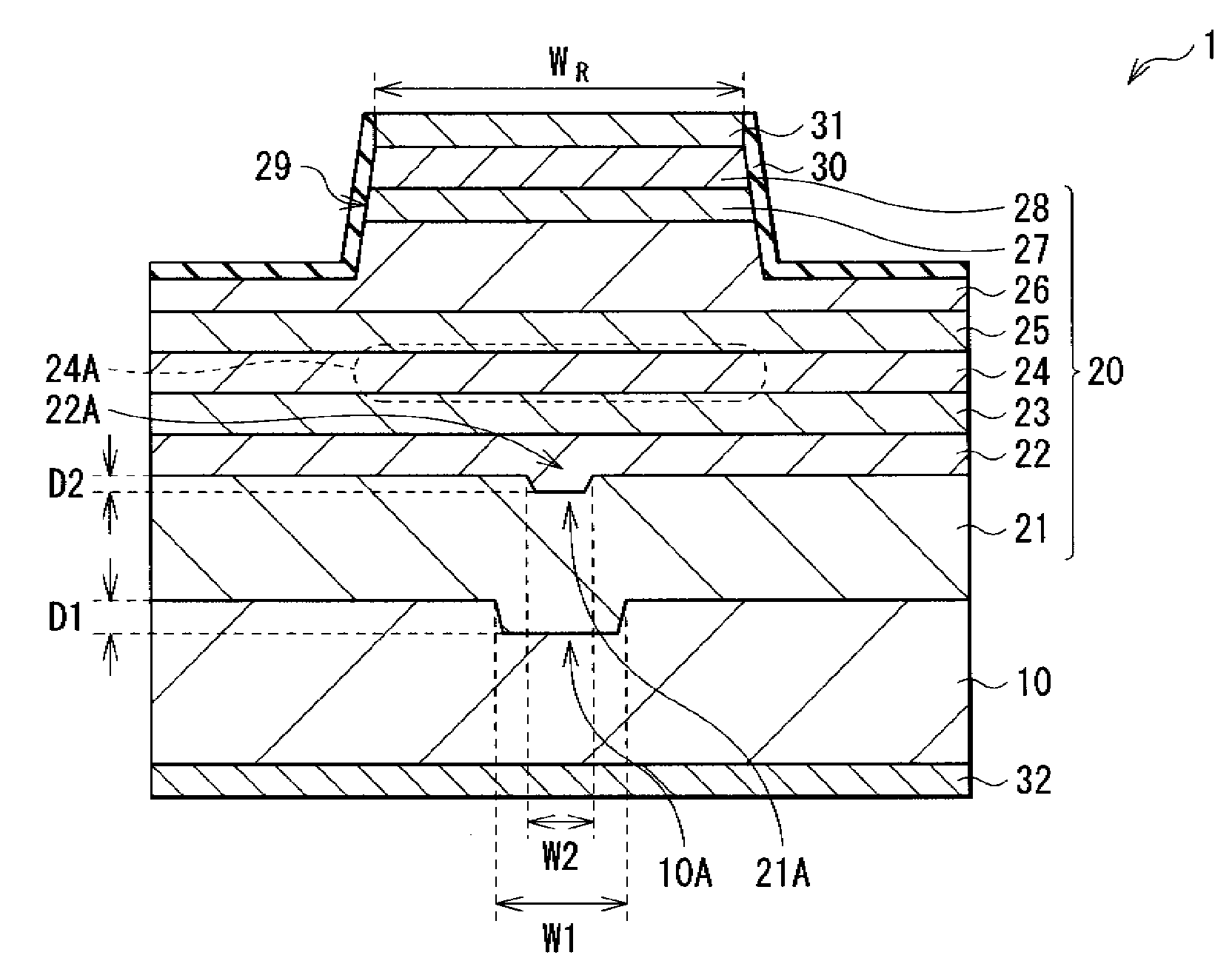
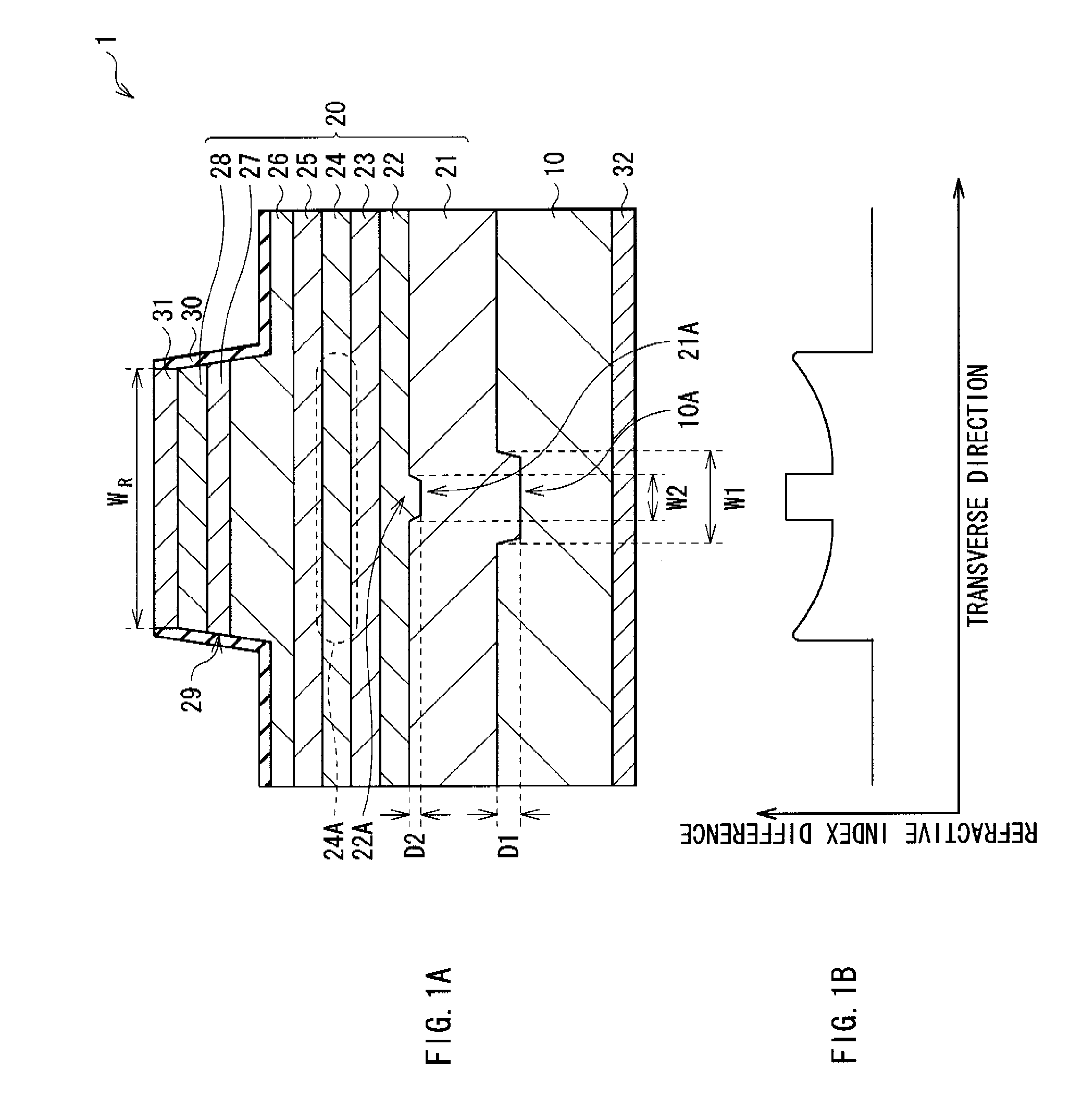
[0069]In the first embodiment, although only one convex portion 22A (the concave portion 21A and the concave portion 10A) is formed, two convex portions 22A may be formed in the central part, for example, as shown in FIG. 4A or three or more convex portions 22A may be formed. In the case where the two convex portions 22A (the concave portions 21A and the concave portions 10A) are formed in the central part, the refractive index distribution is, for example, as shown in FIG. 4B.

[0070]In the first embodiment, although the convex portion 22A is projected to the semiconductor substrate 10 side, the convex portion, instead of the concave portion 10A, may be provided on the semiconductor substrate 10, and the concave portion may be provided corresponding to the convex portion, on the interface of the first lower guide layer 22 on the semiconductor substrate 10 side. In this case, on the interface of the lower cladding layer 21 on the first lower guide layer...

second embodiment

Modification of Second embodiment

[0083]In the second embodiment, the concave portions 33 are formed in the vicinity of both ends in the width direction of the ridge 29, and the narrow-stripe ridge portions 29A and 29C are provided at both ends of the broad-area ridge portion 29B. Thereby, the intensity of the transverse mode in the gain region in the central part and the intensity of the transverse mode in the index region at both ends are in good balance. However, as shown in a laser diode 3 in FIG. 10A, instead of the concave portions 33, a strip-shaped electrode (an upper electrode layer 31) may be provided only on the upper surface of the central part where the ridge portion 29B of the ridge 29 is provided. The refractive index distribution of the laser diode 3 of FIG. 10A is shown in FIG. 10B. Even in this case, the current is actively injected into the gain region in the central part, from the upper electrode layer 31, and the amount of the current injected into the index regi...

third embodiment

Modification of Third Embodiment

[0098]In the third embodiment, although one convex portion 22A (the concave portion 21A and the concave portion 10A) is formed, two or more convex portions 22A may be formed. For example, in the case where the two convex portions 22A are provided as shown in FIG. 16A, a space W1 between the two convex portions 22A may have a width larger than a width (a width of a portion of an upper electrode layer 34 which is in contact with a contact layer 28) of an upper electrode layer 34. FIG. 16B shows a refractive index distribution of the laser diode of FIG. 16A.

[0099]In this case, the width of the transverse mode is defined by the space Wi, and the width of the transverse mode is suppressed from being larger than the space Wi. For example, in the case where the two convex portions 22A are provided, the width of the space Wi between the two convex portions 22A may be almost equal to the width (a width of a portion of the upper electrode layer 34 in contact wi...


PUM


Abstract

Provided is a laser diode which realizes NFP with a stable and uniform shape. The laser diode includes, on a semiconductor substrate, an active layer, one or a plurality of strip-shaped current confinement structures confining a current which is injected into the active layer, and a stacked structure including one or a plurality of strip-shaped convex portions extending in an extending direction of the current confinement structure.

Description

CROSS REFERENCES TO RELATED APPLICATIONS[0001]The present invention contains subject matter related to Japanese Patent Application JP 2007-259429 filed in the Japanese Patent Office on Oct. 3, 2007, the entire contents of which being incorporated herein by reference.BACKGROUND OF THE INVENTION[0002]1. Field of the Invention[0003]The present invention relates to a laser diode having one or a plurality of current confinement structures, and in particular, relates to a broad-area laser diode suitable for high output applications and a method of manufacturing the same.[0004]2. Description of the Related Art[0005]As a compact and low-cost laser light source with high reliability and high output capability, a so-called broad-area laser diode including a waveguide with its width (i.e. stripe width) widened has been utilized in various fields such as displays, printing products, initialization devices of optical disks, fabricating materials, and medical applications. In a typical broad-area...

Claims


Application Information

Patent Timeline
IPC IPC(8): H01S5/02H01L21/02
CPCH01S5/0207H01S5/1064H01S5/1085H01S5/2036H01S2301/206H01S5/22H01S5/2235H01S2301/18H01S5/2054H01S5/20H01S3/0941
Inventor HIRATA, SHOJIASATSUMA, TSUNENORITAKIGUCHI, YOSHIRO
Owner SONY CORP
Why Eureka
Try Eureka