Method for forming an air gap in multilevel interconnect structure

a multi-level interconnect and air gap technology, applied in the direction of coatings, solid-state devices, chemical vapor deposition coatings, etc., can solve the problems of stability problems, multiple problems in the thermal process used in large air gap formation

Inactive Publication Date: 2009-04-09
APPLIED MATERIALS INC
View PDF49 Cites 254 Cited by
  • Summary
  • Abstract
  • Description
  • Claims
  • Application Information

AI Technical Summary

Benefits of technology

[0009]The present invention generally provides methods for forming multilevel interconnect structures, in

Problems solved by technology

However, thermal processes used in large air gap formation have several problems.
For exa

Method used


Image

  • Method for forming an air gap in multilevel interconnect structure
  • Method for forming an air gap in multilevel interconnect structure
  • Method for forming an air gap in multilevel interconnect structure

Examples


example 1

[0037]A PECVD deposition process for depositing a porous dielectric barrier having silicon carbide comprises using a precursor comprising the combination of trimethylsilane (TMS, (CH3)3SiH) and ethylene (C2H4). The process conditions, including the ratio of TMS and ethylene, are set such that the atomic percentage of carbon is greater than 15%. In one embodiment, the ratio of ethylene and TMS is about 1:1 to about 8:1, the flow rate of the TMS / ethylene precursor and carrier gas is between about 5 sccm to about 10,000 sccm, and the temperature is about 350° C. For these conditions, the chamber pressure is between about 10 mTorr to about one atmosphere, the radio frequency (RF) power for plasma generation is between about 15 W to about 3,000 W, and the spacing between a substrate and a shower head, configured for providing precursors to the substrate being processed, is from about 200 mils to about 2000 mils.

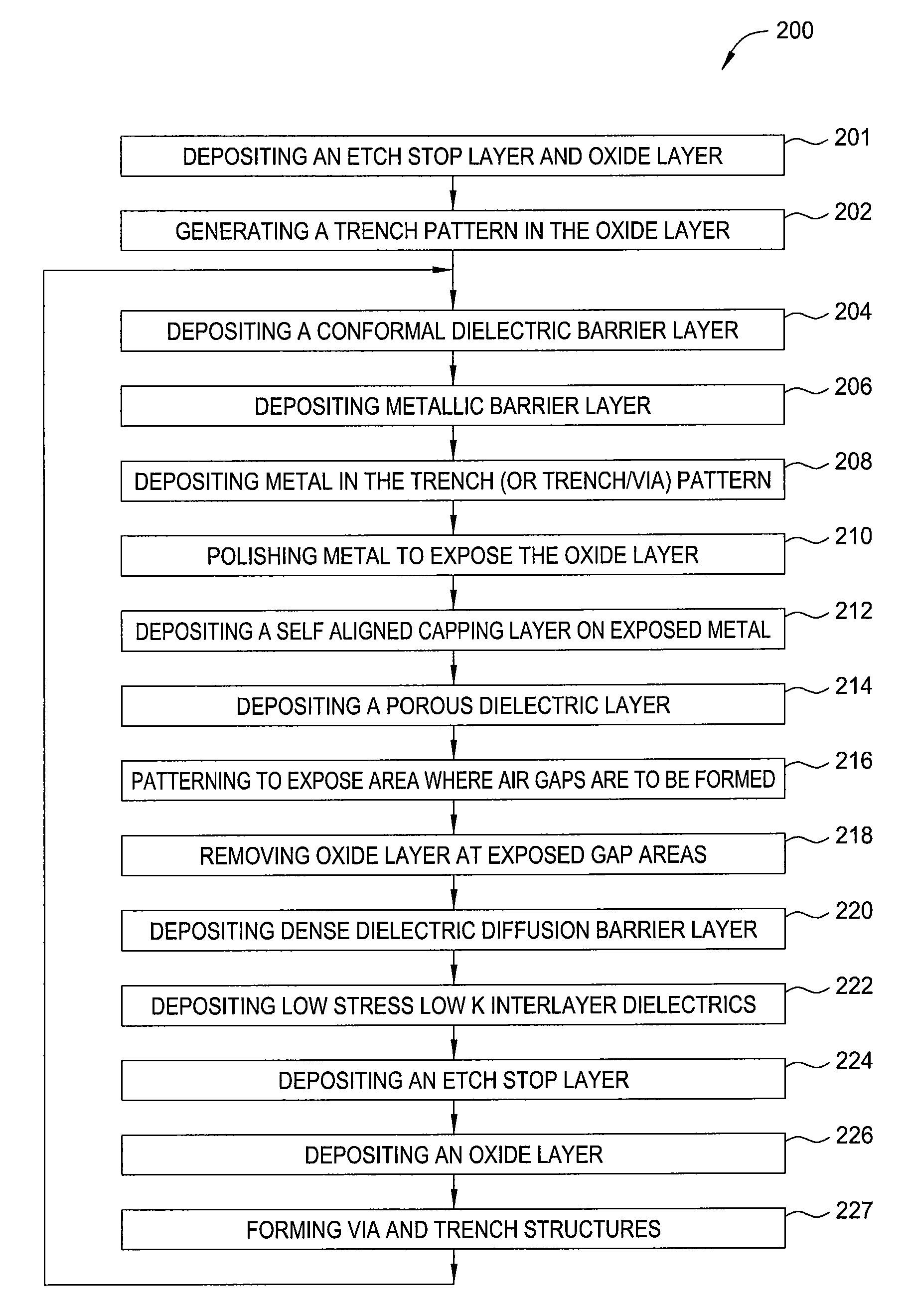
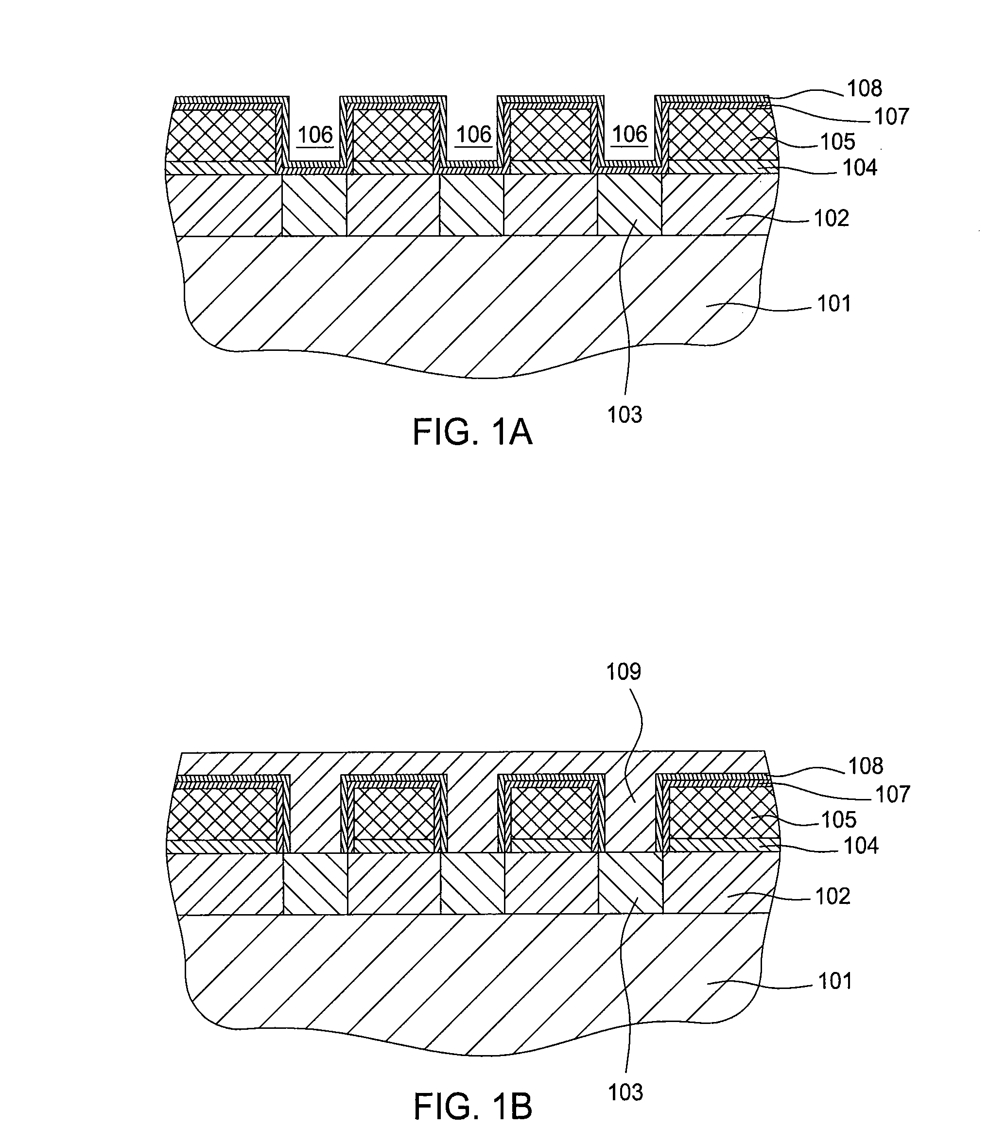
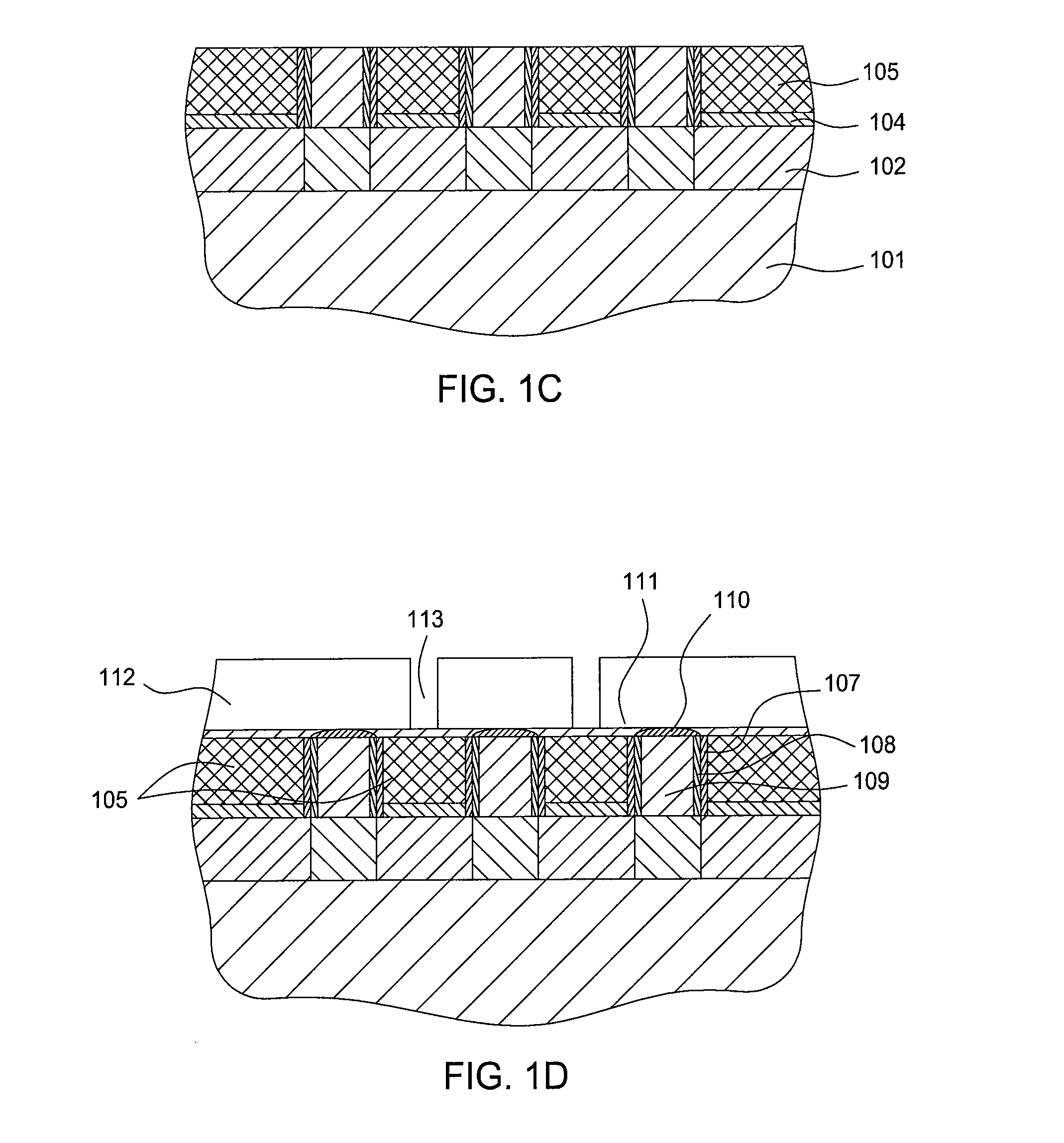
[0038]Returning to FIG. 4, in step 216, a pattern may be generated to expose ...


PUM

PropertyMeasurementUnit
Angleaaaaaaaaaa
Angleaaaaaaaaaa
Thicknessaaaaaaaaaa

Abstract

The present invention generally provides a method for forming multilevel interconnect structures, including multilevel interconnect structures that include an air gap. One embodiment provides a method for forming conductive lines in a semiconductor structure comprising forming trenches in a first dielectric layer, wherein air gaps are to be formed in the first dielectric layer, depositing a conformal dielectric barrier film in the trenches, wherein the conformal dielectric barrier film comprises a low k dielectric material configured to serve as a barrier against a wet etching chemistry used in forming the air gaps in the first dielectric layer, depositing a metallic diffusion barrier film over the conformal low k dielectric layer, and depositing a conductive material to fill the trenches.

Description

BACKGROUND OF THE INVENTION[0001]1. Field of the Invention[0002]Embodiments of the present invention generally relate to the fabrication of integrated circuits. More particularly, embodiments of the present invention relate to methods for forming multilevel interconnect structures that include dielectric materials having low dielectric constants.[0003]2. Description of the Related Art[0004]Integrated circuit geometries have dramatically decreased in size since such devices were first introduced several decades ago. Since then, integrated circuits have generally followed the two year / half-size rule (often called Moore's Law), which means that the number of devices on a chip doubles every two years. Today's fabrication facilities are routinely producing devices having 0.1 μm feature sizes, and tomorrow's facilities soon will be producing devices having even smaller feature sizes.[0005]The continued reduction in device geometries has generated a demand for films having low dielectric c...

Claims


Application Information

Patent Timeline
IPC IPC(8): H01L21/76
CPCC23C16/325H01L21/31144H01L21/3148H01L21/31633H01L21/76804H01L21/76807H01L2221/1036H01L21/76829H01L21/76831H01L21/76832H01L21/76834H01L21/76849H01L21/76885H01L21/7682H01L21/02167H01L21/0217H01L21/02304H01L21/02203H01L21/02274H01L21/02112H01L21/3205H01L21/28
Inventor XIA, LI-QUNXU, HUIWENBALSEANU, MIHAELAWITTY, DEREK R.M'SAAD, HICHEM
Owner APPLIED MATERIALS INC
Why Eureka
Try Eureka