Ultraviolet irradiation method and apparatus using the same

a technology of ultraviolet ray and irradiation method, which is applied in the direction of electrical equipment, adhesives, basic electric elements, etc., can solve problems such as damage to wafers, and achieve the effect of suppressing heat generation and enhancing the intensity of ultraviolet rays

Inactive Publication Date: 2009-04-16
NITTO DENKO CORP
View PDF6 Cites 10 Cited by
  • Summary
  • Abstract
  • Description
  • Claims
  • Application Information

AI Technical Summary

Benefits of technology

[0010]An object of the present invention is to provide an ultraviolet irradiation method and a device using the same capable of evenly curing the adhesive of the ultraviolet curable protective tape to be in a state enabling the protective tape to be separated at satisfactory precision.

Problems solved by technology

However, this method has the following problems.
Furthermore, if the protective tape is separated without the adhesive force of the portion that ran out in the adhesive lowered, excessive separating stress may be concentrated on the wafer edge thereby damaging the wafer, or the adhesive may remain on the wafer edge.

Method used


Image

  • Ultraviolet irradiation method and apparatus using the same
  • Ultraviolet irradiation method and apparatus using the same
  • Ultraviolet irradiation method and apparatus using the same

Examples


Embodiment Construction

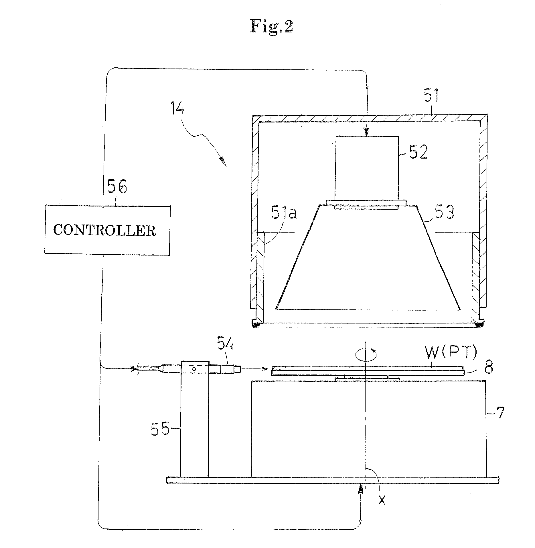
[0046]An embodiment of a semiconductor wafer mount apparatus of the present invention including an ultraviolet irradiation device of the present invention will be described with reference to the drawings.

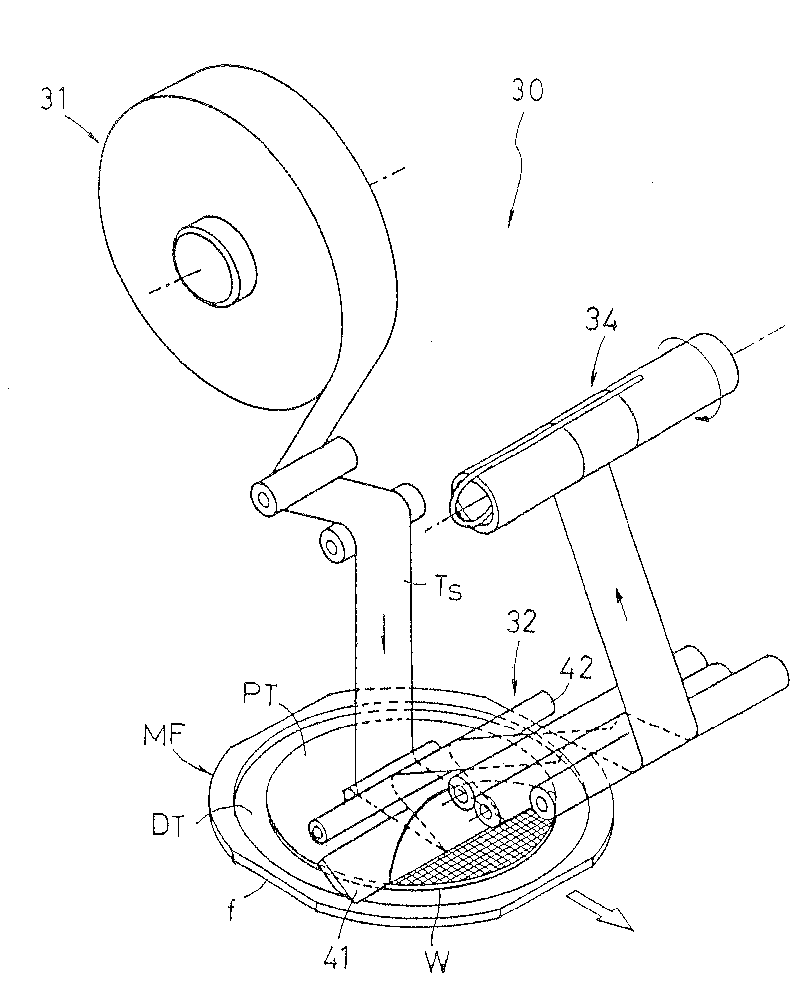
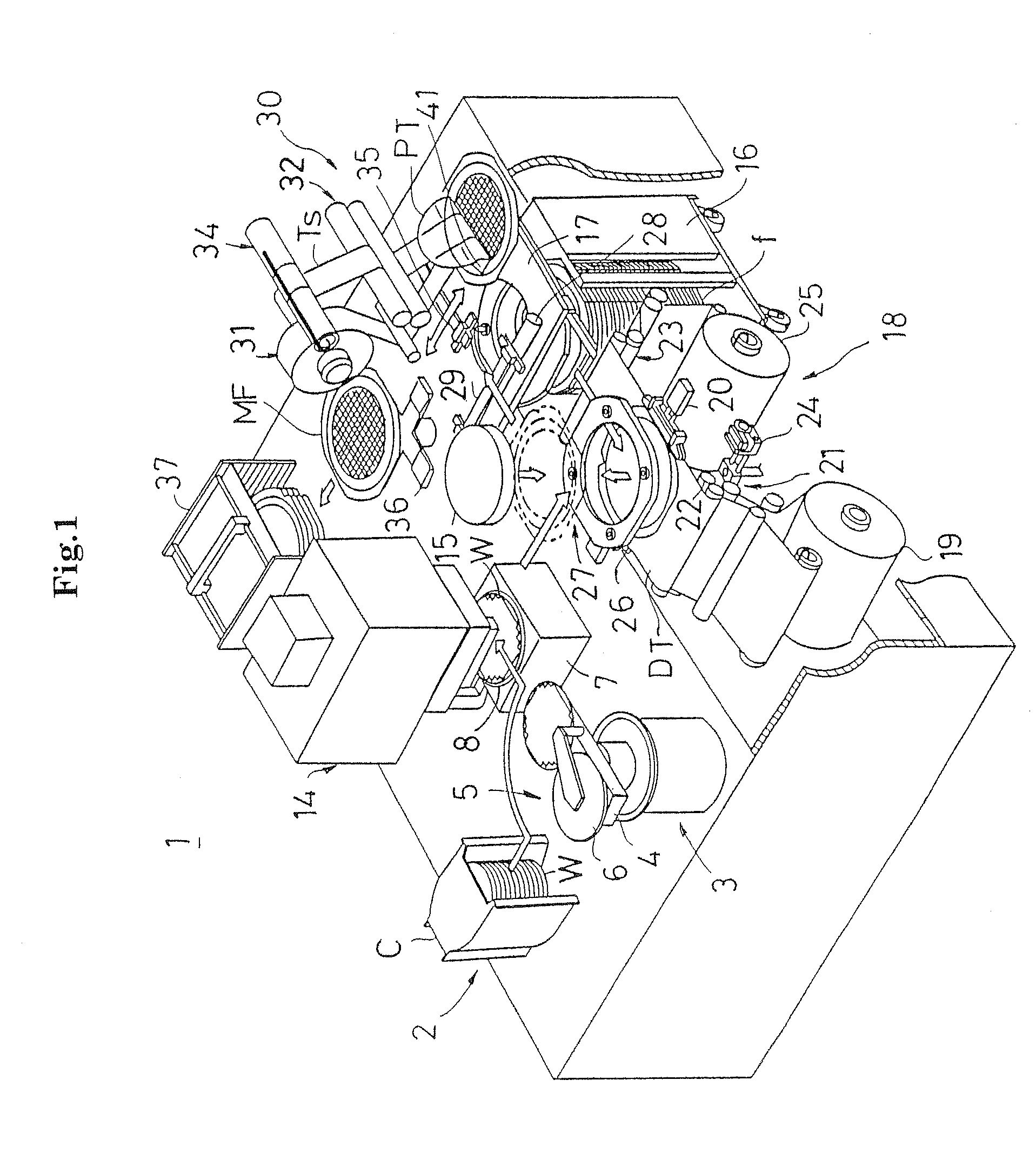
[0047]FIG. 1 is a cutaway perspective view illustrating a whole configuration of a semiconductor wafer mount apparatus according to one embodiment of the invention.

[0048]A semiconductor wafer mount apparatus 1 of the present embodiment includes a wafer supply part 2 in which cassette C for housing semiconductor wafers W (hereinafter, simply referred to as “wafer W”) subjected to a back grinding process in multiple stages are loaded, a wafer transport mechanism 3 having a robot arm 4 and a pressing mechanism 5, an alignment stage 7 for aligning the wafer W, an ultraviolet irradiation unit 14 for applying ultraviolet rays to the wafer W mounted on the alignment stage 7, a chuck table 15 for sucking and holding the wafer W, a ring frame supply part 16 in which ring frames f are housed ...


PUM

PropertyMeasurementUnit
adhesive forceaaaaaaaaaa
unit areaaaaaaaaaaa
areaaaaaaaaaaa

Abstract

The ultraviolet ray is applied on the surface of the protective tape from an ultraviolet ray generator. In addition, the ultraviolet ray having intensity higher than that from the ultraviolet ray generator is applied on spot on the wafer edge by an irradiation gun. In this case, the ultraviolet ray intensity and the rotation speed of the holding table are controlled by a controller so that the ultraviolet irradiation amount per unit area of the wafer edge portion becomes equal to that to the joining surface of the protective tape.

Description

BACKGROUND OF THE INVENTION[0001](1) Field of the Invention[0002]The present invention relates to an ultraviolet irradiation method and a device using the same for irradiating a protective tape with ultraviolet ray and lowering an adhesive force thereof before separating an ultraviolet curable protective tape joined to a surface of a semiconductor wafer.[0003](2) Description of the Related Art[0004]A semiconductor wafer (hereinafter, simply referred to as “wafer”) is thinned by processing the back side of the wafer by using a mechanical method such as sharpening or grinding or a chemical method using etching. At the time of processing the wafer by using any of the methods, a protective tape is joined to a surface of the wafer to protect the surface on which a wiring pattern is formed. The wafer to which the protective tape is joined and which is grinded is arranged at the center of a ring frame, and a supporting adhesive tape is joined over the ring frame and the back side of the wa...

Claims


Application Information

Patent Timeline
Patent Type & Authority Applications(United States)
IPC IPC(8): B29C71/04
CPCH01L21/67132Y10T156/1158Y10T156/19
Inventor YAMAMOTO, MASAYUKIHASE, YUKITOSHIMATSUSHITA, TAKAOKANESHIMA, YASUJI
Owner NITTO DENKO CORP
Why Eureka
Try Eureka