Optical device and manufacturing method thereof and semiconductor device

a manufacturing method and semiconductor technology, applied in semiconductor devices, solid-state devices, television systems, etc., can solve the problems of defective semiconductor devices, more disadvantageous optical devices in heat release efficiency, and failure of control circuits, so as to improve overall heat release efficiency of semiconductor elements, prevent defective semiconductor devices, and improve the effect of overall heat release efficiency

Active Publication Date: 2009-04-16
PANNOVA SEMIC
View PDF4 Cites 26 Cited by
  • Summary
  • Abstract
  • Description
  • Claims
  • Application Information

AI Technical Summary

Benefits of technology

[0038]In the semiconductor device according to the one aspect of the invention, a heat release path from the semiconductor element to the thin plate body can be ensured by providing the thin plate body over the back surface of the semiconductor element. As a result, the overall heat release efficiency of the semiconductor element can be improved by using a contact region with another member, that is, the thin plate body.
[0039]Moreover, the base is hermetically sealed by the thin plate body provided under the base with the semiconductor element interposed therebetween. Therefore, dust, water and the like can be prevented from entering from the outside, and a defective semiconductor device can be prevented from being caused by adhesion of dust, water, and the like.
[0040]Moreover, an efficient heat release path is formed from the semiconductor element to the external terminals through a metal having high thermal conductivity efficiency. Especially, since the bumps are provided between the leads and the electrode pads, the thermal conductivity efficiency can be improved as compared to a conventional example in which thin long gold wires are provided.
[0041]As described above, in the optical device and the manufacturing method according to the invention, a heat release path from the optical element to the thin plate body can be ensured by providing the thin plate body over the back surface of the optical element. As a result, the overall heat release efficiency of the optical element can be improved by using a contact region with another member, that is, the thin plate body. Moreover, an optical device compatible with an existing surface-mounting type optical device can be implemented.
[0042]In the semiconductor device according to the invention, a heat release path from the semiconductor element to the thin plate body can be ensured by providing the thin plate body over the back surface of the semiconductor element. As a result, the overall heat release efficiency of the semiconductor element can be improved by using a contact region with another member, that is, the thin plate body.

Problems solved by technology

Especially optical devices need to have an optical path above an optical element, and a heat releasing member cannot be provided above the optical element.
Therefore, the structure of the optical devices is more disadvantageous in terms of heat release efficiency as compared to other semiconductor devices.
With recent increase in the heat generation amount in the control circuit, however, there has been a recognized concern that the above heat release path is not enough to release the heat generated in the control circuit, and high temperature in the control circuit region may cause malfunction or breakdown of the control circuit.
However, the conventional optical device has the following problem:
In other words, a sufficient heat release path cannot be ensured for the overall heat generation in the optical element, causing degradation in the overall heat release efficiency of the optical element.
The same problem also occurs in a hollow-type semiconductor device having a semiconductor element mounted thereon and having the same structure as that of the above optical device.
In other words, a sufficient heat release path cannot be ensured for the overall heat generation in the semiconductor element, causing degradation in the overall heat release efficiency of the semiconductor element.

Method used


Image

  • Optical device and manufacturing method thereof and semiconductor device
  • Optical device and manufacturing method thereof and semiconductor device
  • Optical device and manufacturing method thereof and semiconductor device

Examples


first embodiment

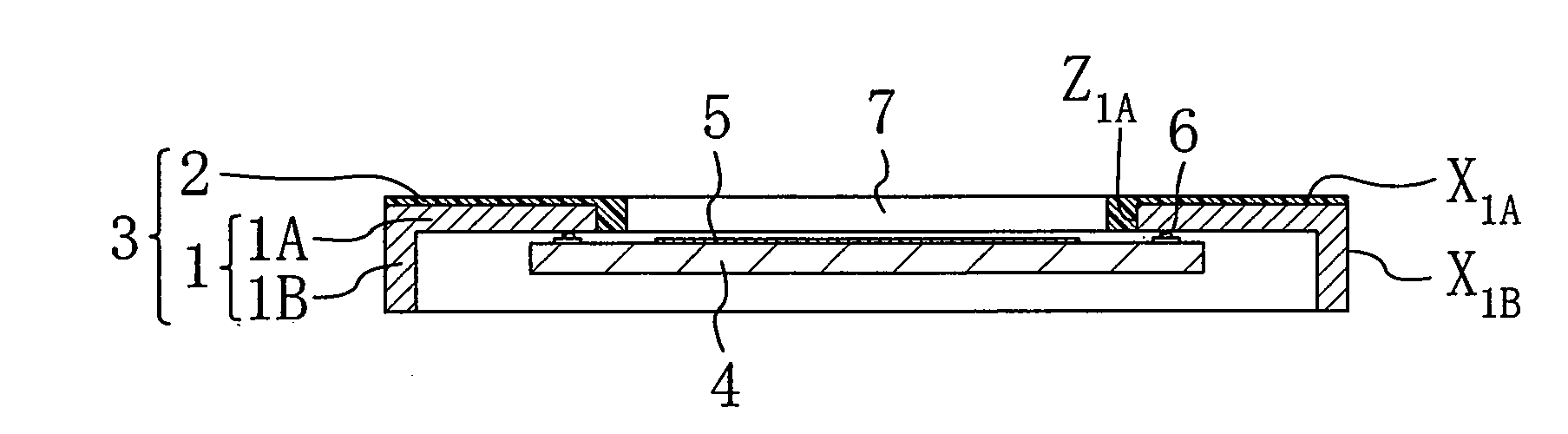
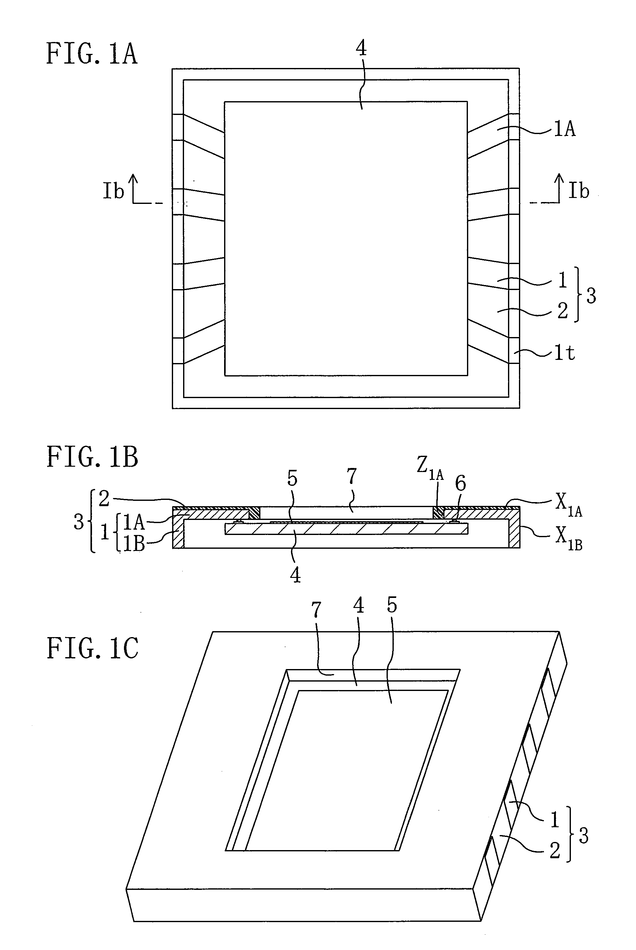
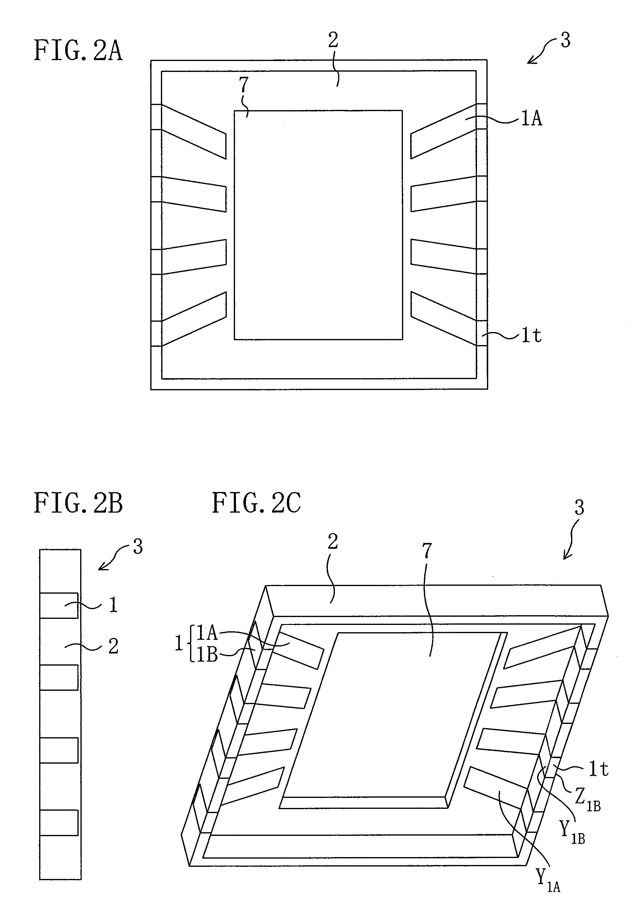
[0056]Hereinafter, an optical device according to a first embodiment of the invention will be described with reference to FIGS. 1A through 1C. FIGS. 1A through 1C are diagrams showing a structure of the optical device of the first embodiment. FIG. 1A is a plan view of the optical device when viewed from the back side of an optical element. FIG. 1B is a cross-sectional view taken along line Ib-Ib in FIG. 1A. FIG. 1C is a perspective view of the optical device when viewed from the front side of the optical element.

[0057]As shown in FIG. 1B, the optical device of this embodiment mainly includes a base 3 and an optical element 4. The base 3 has a through hole 7 in the center and includes leads 1 and a resin 2. The optical element 4 is provided under the base 3 so as to correspond to the through hole 7, and has a light detecting region 5 in the center. The leads 1 of the base 3 are respectively connected to electrode pads on the optical element 4 through bumps 6.

[0058]As shown in FIG. 1B...

second embodiment

[0069]Hereinafter, an optical device according to a second embodiment of the invention will be described with reference to FIG. 3. FIG. 3 is a cross-sectional view showing a structure of the optical device of the second embodiment.

[0070]As shown in FIG. 3, the optical device of this embodiment further includes a thin plate body 8 and a transparent member 10 in addition to the structure of the first embodiment. The thin plate body 8 is provided under the optical element 4 through a bonding member 9, and the transparent member 10 is provided in the through hole of the base 3 through an adhesive 11.

[0071]The thin plate body 8 has a thickness of, for example, 200 μm to 400 μm. The thin plate body 8 is made of, for example, ceramic. The thin plate body 8 may alternatively be made of other materials such as a metal plate. For example, an adhesive is used as the bonding member 9. Other materials such as an adhesive sheet may alternatively be used as the bonding member 9.

[0072]The transpare...

third embodiment

[0108]Hereinafter, a camera module according to a third embodiment of the invention (a camera module including the optical device of the invention) will be described. A camera module including the optical device of the first modification of the second embodiment will be described below as an example. FIG. 9 is a cross-sectional view showing a structure of the camera module of the third embodiment.

[0109]The “camera module” herein indicates various types of equipments such as a digital still camera, a mobile phone camera, a video camera with mobile phone, an on-board camera, a surveillance camera, a video camera, a medical camera, a broadcast camera, a webcam, a camera with video phone, a game camera, an optical mouse, a DVD (Digital Versatile Disc) drive, and a CD (Compact Disc) drive. Note that when the optical device of the invention is used in the camera module, the optical element of the optical device is a light receiving element such as an image sensor.

[0110]As shown in FIG. 9,...


PUM


Abstract

An optical device includes a base and an optical element. The base has a through hole in a center and includes leads and a resin. Each lead has an L-shaped cross-section and is formed by an inner lead extending from the center toward a peripheral edge and an outer lead connected to the inner lead and extending downward. The optical element is provided under the base so as to correspond to the through hole. Electrode pads of the optical element are connected to the leads of the base through bumps, respectively. The resin is formed so as to cover respective inner ends of the leads and respective front surfaces of the inner leads and to fill a gap between adjacent leads, and respective outer ends of the leads and respective front surfaces of the outer leads are exposed.

Description

CROSS REFERENCE TO RELATED APPLICATIONS[0001]This application claims priority under 35 U.S.C. §119 on Patent Application No. 2007-266447 filed in Japan on Oct. 12, 2007 and Patent Application No. 2008-135535 filed in Japan on May 23, 2008, the entire contents of which are hereby incorporated by reference.BACKGROUND OF THE INVENTION[0002]1. Field of the Invention[0003]The invention relates to an optical device on which an optical element for emitting or receiving light is mounted and a manufacturing method thereof, and a camera module having the optical device mounted thereon.[0004]2. Related Art[0005]With recent improvement in capability of semiconductor devices, the amount of heat that is generated in the semiconductor devices has been increasing, and improvement in heat release efficiency of the semiconductor devices has been greatly demanded. Especially optical devices need to have an optical path above an optical element, and a heat releasing member cannot be provided above the ...

Claims


Application Information

Patent Timeline
Patent Type & Authority Applications(United States)
IPC IPC(8): H01L31/0232H01L21/62
CPCH01L27/14618H04N5/2257H01L27/14685H01L27/14625H01L2224/73253H04N23/57
Inventor MATSUMOTO, KATSUYOSHI
Owner PANNOVA SEMIC
Why Eureka
Try Eureka