Semiconductor device

Active Publication Date: 2009-04-16
MITSUBISHI ELECTRIC CORP
View PDF0 Cites 17 Cited by
  • Summary
  • Abstract
  • Description
  • Claims
  • Application Information

AI Technical Summary

Benefits of technology

[0009]The present invention has been made to solve the above problems. It is therefore an object of the present invention to provide a sem

Problems solved by technology

When the upper arm and the lower arm are both on, a short circuit (arm short-circuit) occurs between the upper arm and the lower arm, so that a short-circuit current flows, thus producing bad influences such as characteristic degradation of the upper and lower arms.
Thus, the power conversion

Method used


Image

  • Semiconductor device
  • Semiconductor device
  • Semiconductor device

Examples


first embodiment

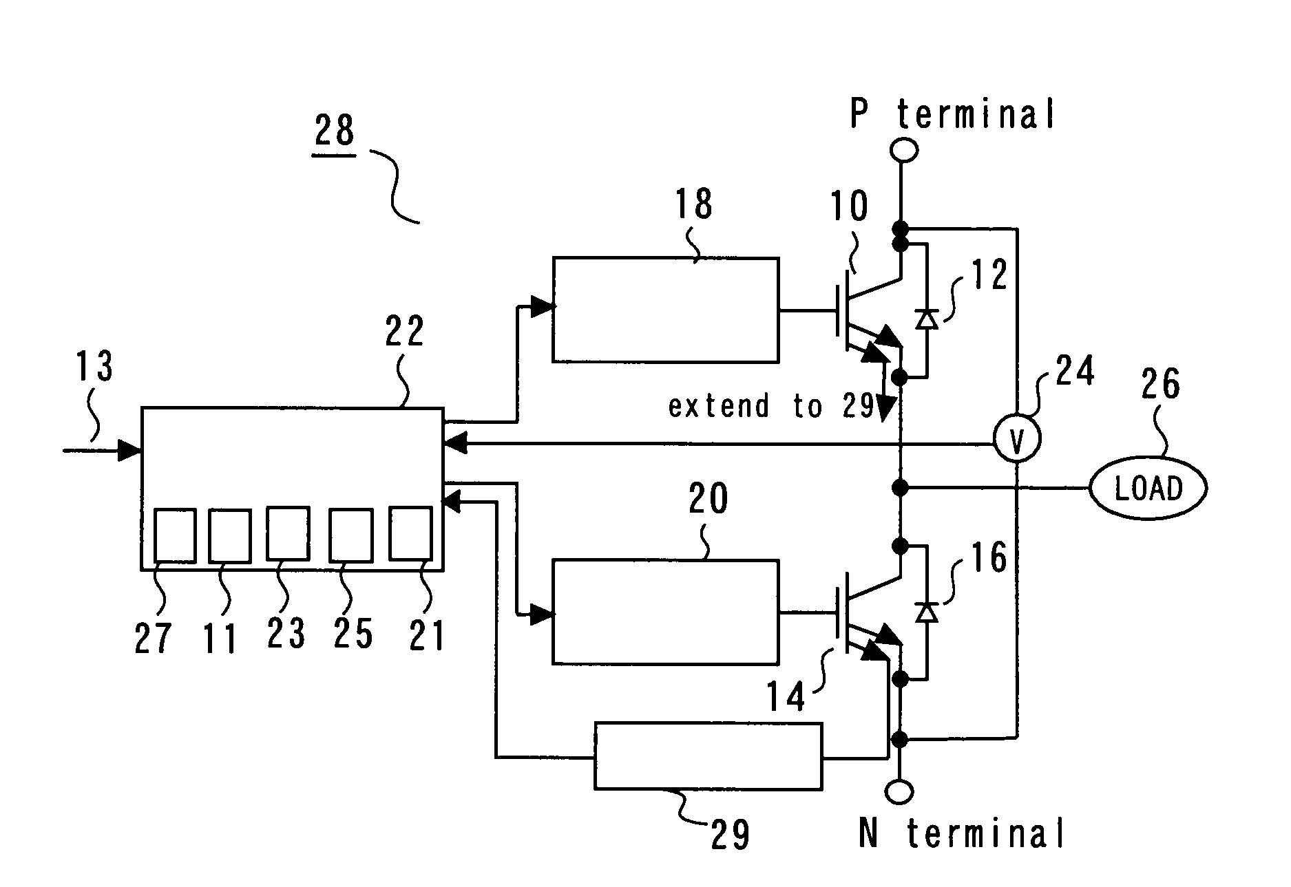
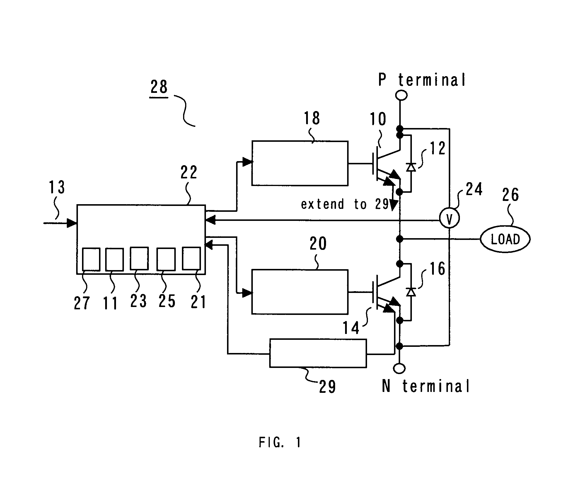
[0025]The present invention relates to a semiconductor device capable of generating optimum dead time by simple processing. The semiconductor device according to the present embodiment has such a configuration as shown in FIG. 1. FIG. 1 will be explained subsequently. The semiconductor device 28 is equipped with a first semiconductor element 10 and a second semiconductor element 14. The first semiconductor element 10 and the second semiconductor element 14 form a half bridge circuit. The first semiconductor element 10 and the second semiconductor element 14 may be generically called arms subsequently.

[0026]The first semiconductor element 10 and the second semiconductor element 14 that constitute the arms correspond to power switching elements. As the power switching elements, may be mentioned, for example, IGBTs (Insulated Gate Bipolar Transistors) and power MOSFETs. A backflow diode 12 is connected in parallel to the first semiconductor element 10. A backflow diode 16 is connected ...

second embodiment

[0053]The present embodiment relates to a semiconductor device capable of attaining a desired actual control value in the semiconductor device to which the dead time is set. A semiconductor control system according to the present embodiment is provided with such a configuration as shown in FIG. 9. The semiconductor control system 70 according to the present embodiment can be divided broadly into a semiconductor device 72 and a host system 78. Here, the semiconductor device 72 will be regarded as identical to the semiconductor device 28 shown in FIG. 1, which has been described in the first embodiment.

[0054]On the other hand, the host system 78 is of a control value transmitting circuit which sends a control value to be realized by the semiconductor device 72. The host system 78 includes a control device 76 and a dead time compensating section 74. The control device 76 is a device which transmits a signal for controlling the semiconductor device 72 to the dead time compensating secti...


PUM


Abstract

The present invention provides a semiconductor device includes arms formed by two semiconductor elements, a map memory device which stores therein a correlation map between a control value for each of the arms and an optimized dead time to be set for the control value or is capable of storing the same therein, drive control value acquiring means for acquiring a drive control value of each of the arms, and a dead time generating circuit for extracting the optimized dead time corresponding to the drive control value from the correlation map. The time taken until the other of the semiconductor elements is turned on after one thereof has received a command to turn off the same is the optimized dead time extracted by the dead time generating circuit.

Description

BACKGROUND OF THE INVENTION[0001]1. Field of the Invention[0002]The present invention relates to a semiconductor device which sets dead time to control each semiconductor element, and particularly to a semiconductor device capable of easily determining dead time optimum for a semiconductor element and maintaining a stable control state.[0003]2. Background Art[0004]There are known semiconductor switches formed by configurations called arms, in which two semiconductor elements are arranged vertically. In the configurations, the semiconductor element on the upper side is called upper arm, and the semiconductor element on the lower side is called lower arm. When the upper arm and the lower arm are both on, a short circuit (arm short-circuit) occurs between the upper arm and the lower arm, so that a short-circuit current flows, thus producing bad influences such as characteristic degradation of the upper and lower arms.[0005]Such an arm short-circuit is caused by turning on of the lower ...

Claims


Application Information

Patent Timeline
IPC IPC(8): H03K17/28
CPCH02M1/38H03K17/165H03K17/0828H02M2001/385H02M1/385
Inventor MIYAMOTO, NOBORUTSUJI, NATSUKI
Owner MITSUBISHI ELECTRIC CORP
Why Eureka
Try Eureka