Method of fabricating a flash memory

a technology of flash memory and fabrication method, which is applied in the direction of basic electric elements, electrical apparatus, semiconductor devices, etc., can solve the problems of failure to program or defect flash memory, split-gate flash memory fabricated according to the prior art usually have disadvantages, less stability, and short lifetime, so as to improve the memory performance

Inactive Publication Date: 2009-04-16
POWERCHIP SEMICON CORP
View PDF7 Cites 20 Cited by
  • Summary
  • Abstract
  • Description
  • Claims
  • Application Information

AI Technical Summary

Benefits of technology

[0009]It is an advantage of the claimed invention that an epitaxial layer is formed on the surface of the semiconductor substrate to planarize the surface of the semiconductor substrate before forming the source, such that the following-formed elements, such as the erase gate or the erase-gate insulating layer, can be fabricated above the surface of the semiconductor substrate. As a result, the problems such as point discharge effect in the prior art caused by forming elements in a recess or trench of the substrate can be effectively solved, which may improve the performance of the memory.

Problems solved by technology

Therefore, the following formed second dielectric layer and erase gate will be formed in the AA trenches, easily causing point discharge effect in the AA trenches when the flash memory is under operation, which brings the failure of programming or defects of the flash memory.
As a result, the split-gate flash memories fabricated according to the prior art usually have disadvantages of less stability and short lifetime.

Method used


Image

  • Method of fabricating a flash memory
  • Method of fabricating a flash memory
  • Method of fabricating a flash memory

Examples


Embodiment Construction

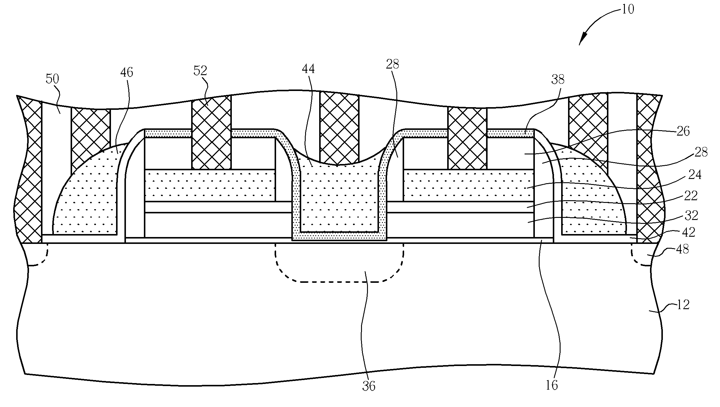
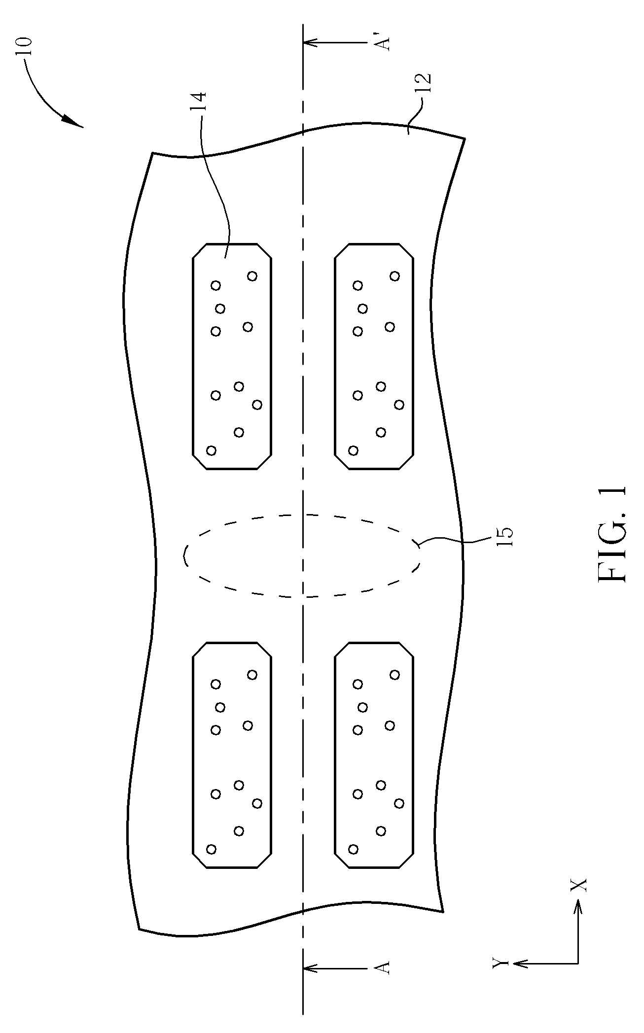
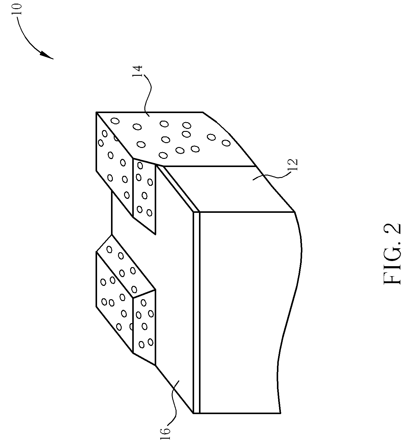
[0012]FIGS. 1-15 are schematic diagrams of a preferable embodiment of the method of fabricating a split-gate flash memory according to the present invention, while FIG. 1 is a top-view diagram; FIGS. 2-11 and FIG. 14 are three-dimensional (3D) diagrams of the sectional view along the Y-direction in FIG. 1; and FIGS. 12, 13 and 15 are sectional views along the X-direction in FIG. 1. As shown in FIG. 1, when fabricating the present invention split-gate flash memory 10, a semiconductor substrate 12 is provided at first, wherein the semiconductor substrate 12 comprises a plurality of STIs 14 thereon. The semiconductor substrate 12 may be a silicon substrate, a P-type substrate, or an N-type substrate. The portion positioned between adjacent STIs 14 along the Y-direction, for example the portion marked by the dotted line, is defined as an active area 15 of the split-gate flash memory 10. Referring to FIG. 2, a dry oxidation process is performed to form an oxide layer on the surface of th...


PUM


Abstract

A method of fabricating a flash memory includes providing a semiconductor substrate with STIs and an active area between two adjacent STIs along a first direction; successively forming a floating-gate insulating layer, a conductive layer, a dielectric layer, a control gate, and a cap layer on the semiconductor substrate; forming spacers on the sidewalls of the cap layer and the control gate; removing the dielectric layer, the conductive layer, and the floating-gate insulating layer not covered by the spacers and the cap layer; performing a selective epitaxial growth process to form an epitaxial layer on the exposed semiconductor substrate in the active area; and forming a source in the epitaxial layer and the semiconductor substrate in the active area.

Description

BACKGROUND OF THE INVENTION[0001]1. Field of the Invention[0002]The invention relates to a fabrication method of a flash memory, and more particularly, to a fabrication method by employing a selective epitaxial growth (SEG) process of a flash memory to improve the performance thereof.[0003]2. Description of the Prior Art[0004]Nonvolatile memories have the advantages of maintaining stored data while the power supply is interrupted, thus have been widely applied to information products. According to the bit numbers stored by a single memory cell, nonvolatile memories are divided into single-bit storage nonvolatile memories and dual-bit storage nonvolatile memories, wherein the former contains nitride read-only-memory (NROM), metal-oxide-nitride-oxide-silicon (MONOS) memories, and silicon-oxide-nitride-oxide-silicon (SONOS) memories, and the latter contains split-gate SONOS memories and split-gate MONOS memories. Comparing to the traditional single-bit storage nonvolatile memories, eac...

Claims


Application Information

Patent Timeline
Patent Type & Authority Applications(United States)
IPC IPC(8): H01L21/3205
CPCH01L27/11521H01L29/7881H01L29/42328H10B41/30
Inventor LIU, MICHAEL-YKUO, HUI-HUNGHSU, HUI-MIN
Owner POWERCHIP SEMICON CORP
Why Eureka
Try Eureka