

Semiconductor memory device with variable resistance element
- Summary
- Abstract
- Description
- Claims
- Application Information
AI Technical Summary
Benefits of technology
Problems solved by technology
Method used
Image

Examples
Embodiment Construction
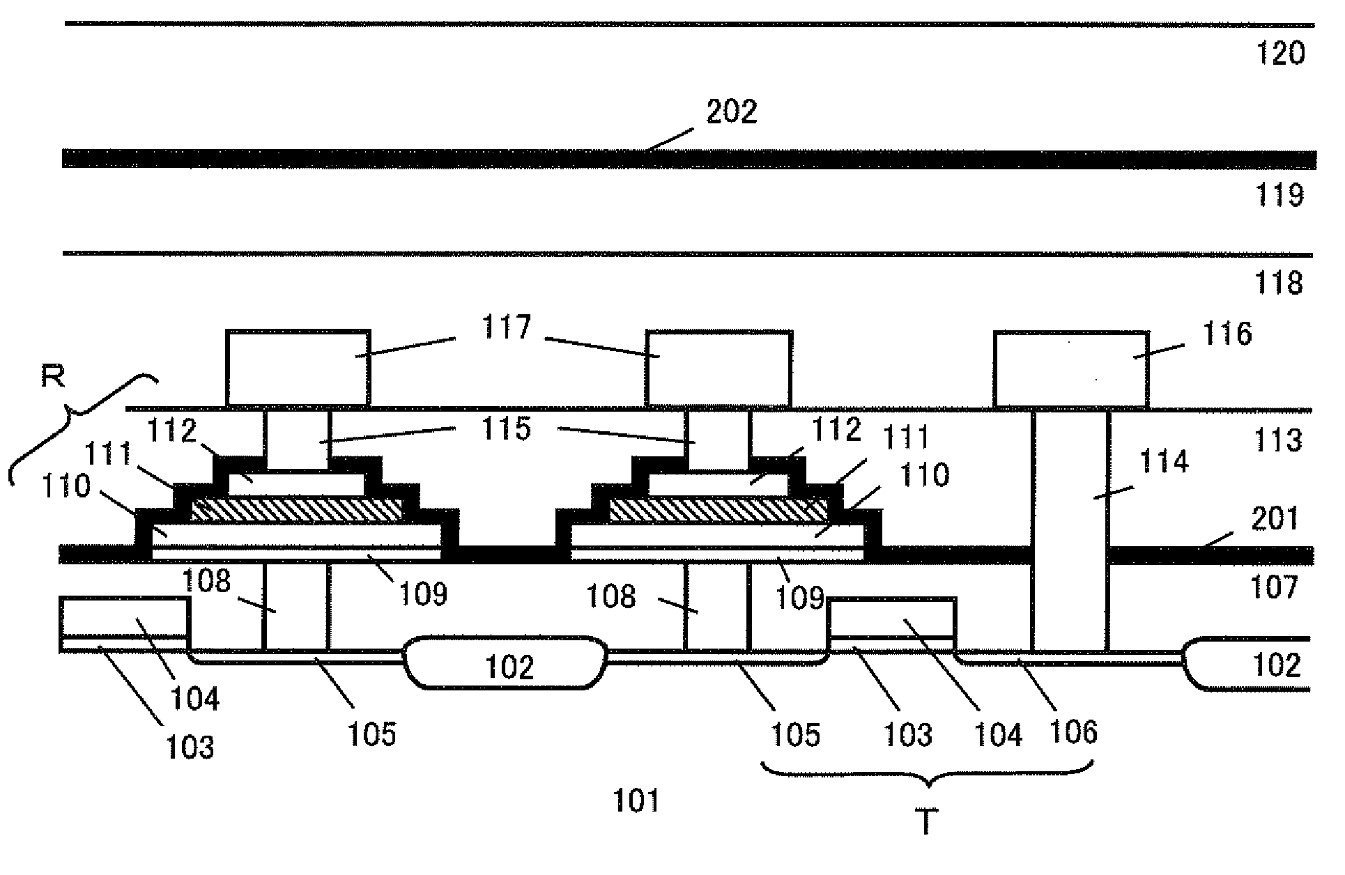
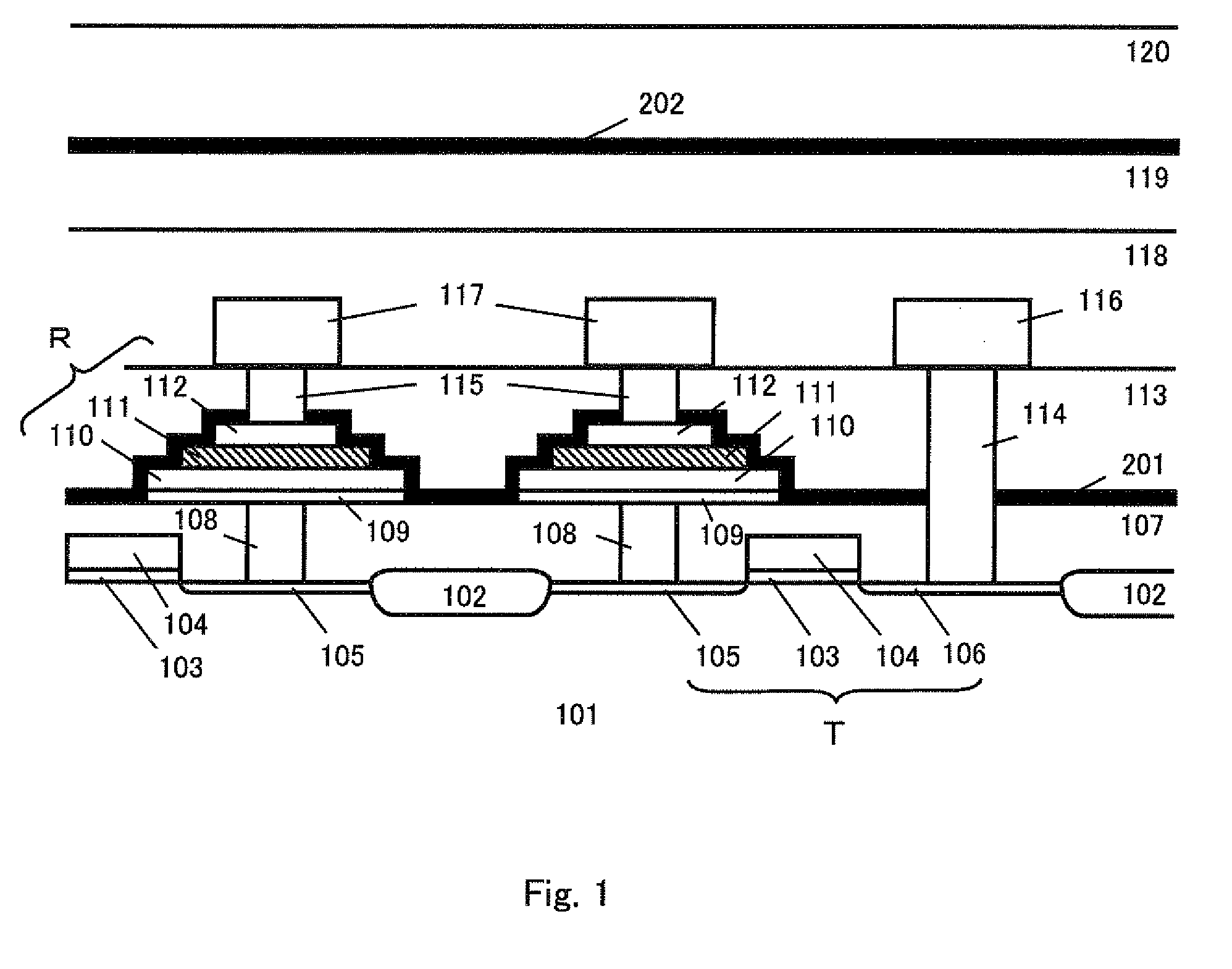
[0072]Hereinafter, embodiments of the semiconductor memory device according to the present invention is explained with reference to figures. A schematic cross-sectional drawing of the resistive semiconductor memory device equipped with a variable resistance element of the present invention is shown in FIG. 1. In the semiconductor memory device of the embodiment of the present invention, the reaction preventing films 201 and 202 are added to the conventional resistive semiconductor memory device shown in FIG. 17. That is, the reaction preventing film 201 is arranged on the variable resistance element R and the reaction preventing film 202 is arranged directly under the passivation film 120. The reaction preventing film 201 prevents an invasion of hydrogen that is a reduction species or oxygen that is an oxidation species into the variable resistance element R, and the reaction preventing film 202 has a function of preventing diffusion of hydrogen that is a reduction species from the ...
PUM
 Abstract
Description
Claims
Application Information