Multi-domain vertical alignment display panel and color filter substrate
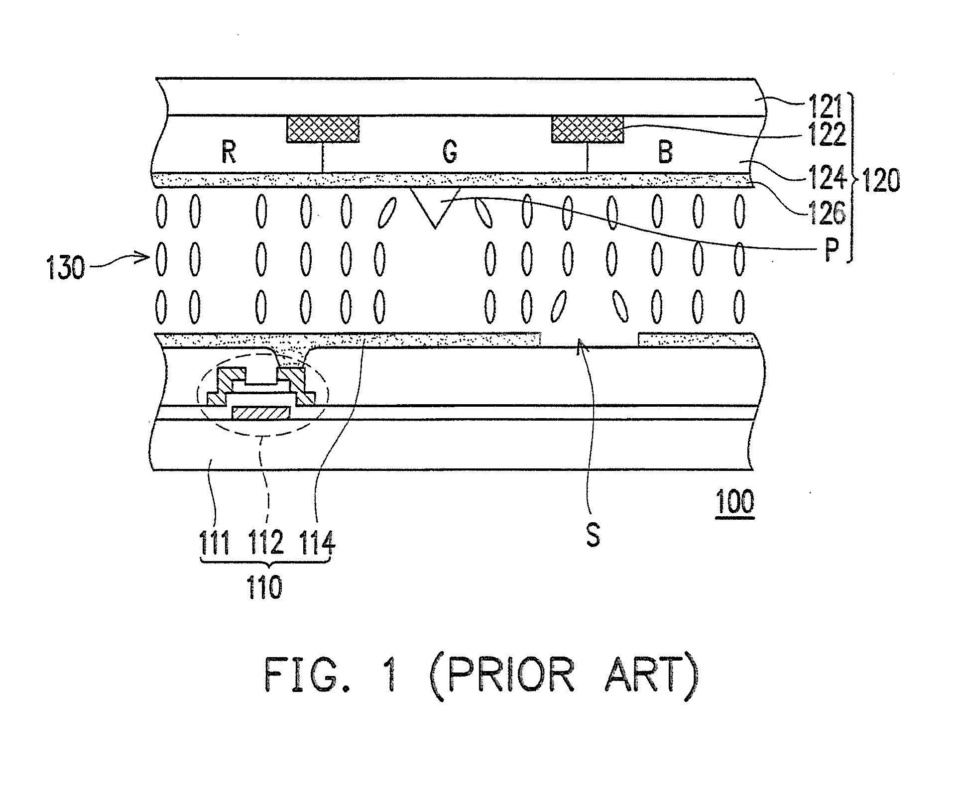
a display panel and color filter technology, applied in the field of display panels and color filter substrates, can solve problems such as abnormal light leakage of display images, and achieve the effect of reducing the manufacturing cost of color filter substrates
- Summary
- Abstract
- Description
- Claims
- Application Information
AI Technical Summary
Benefits of technology
Problems solved by technology
Method used
Image
Examples
first embodiment
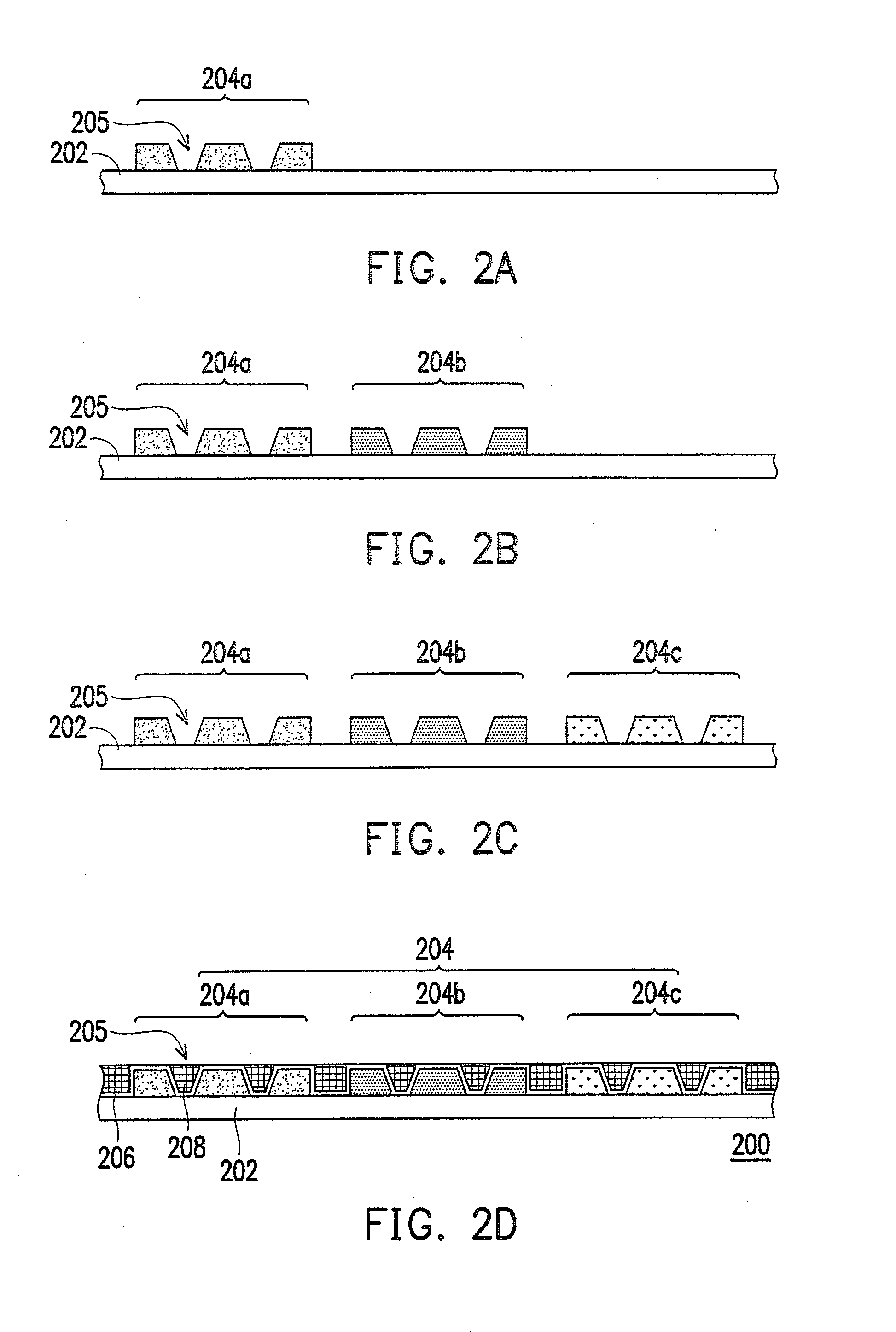
[0027]FIGS. 2A through 2D are schematic cross-sectional flowcharts illustrating a fabricating method of a color filter substrate according to the present invention. First, referring to FIG. 2A, a base 202 is provided. Next, a first patterned filter film layer 204a is formed on the base 202 by performing a photomask process. Here, the first patterned filter film layer 204a has a plurality of recesses 205. Specifically, a material of the first patterned filter film layer 204a is red resin, for example.
[0028]Next, referring to FIG. 2B, a second patterned filter film layer 204b is formed on the base 202 by performing another photomask process. Here, the second patterned filter film layer 204b has a plurality of the recesses 205. A material of the second patterned filter film layer 204b is, for example, green resin.
[0029]After that, referring to FIG. 2C, a third patterned filter film layer 204c is formed on the base 202. Here, the third patterned filter film layer 204c has a plurality of...
second embodiment
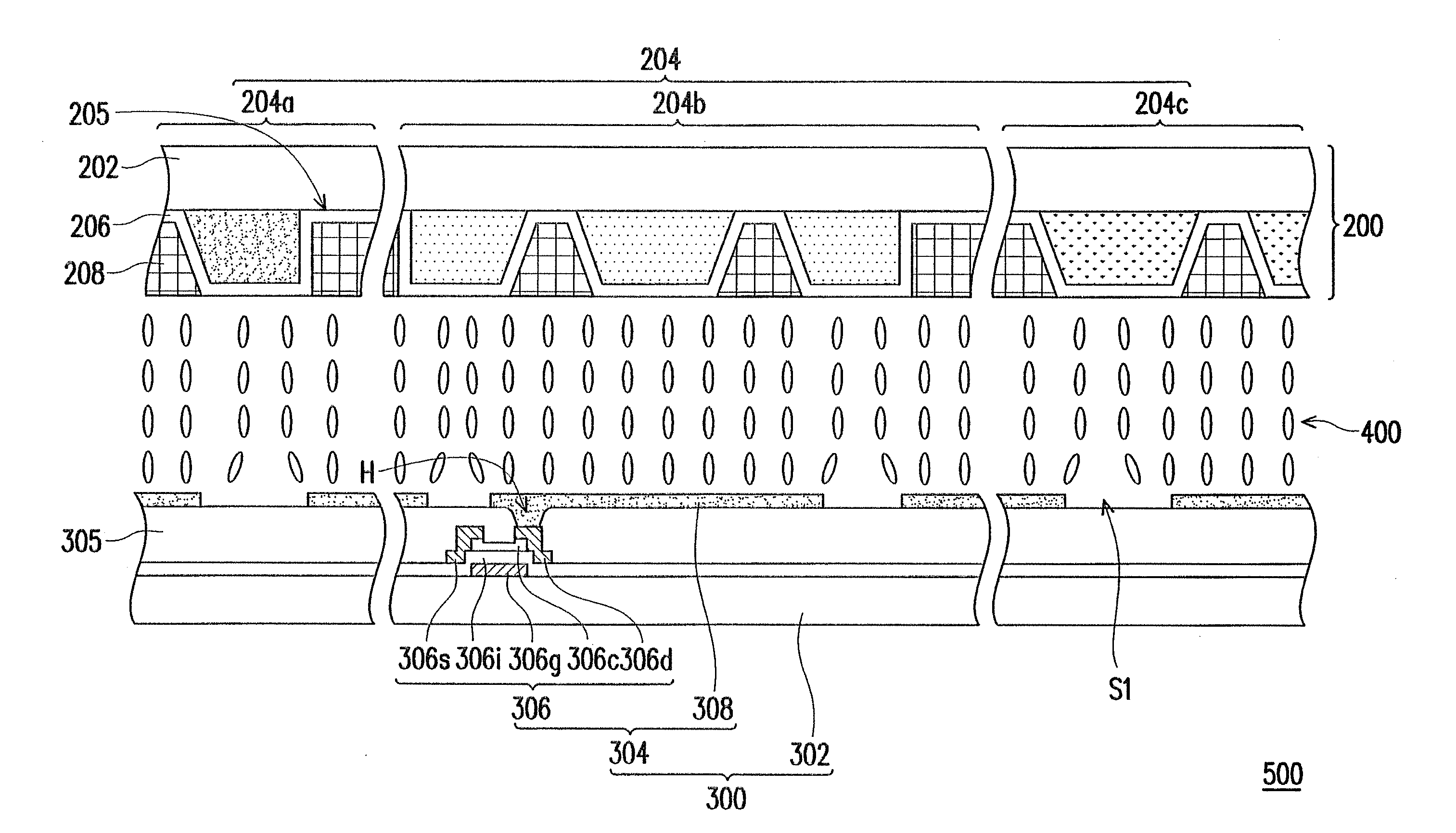
[0035]FIG. 3 is a schematic cross-sectional view depicting a MVA display panel according to the present invention. Referring to FIG. 3, the color filter substrate 200 and a MVA active device array substrate 300 are provided. The description of the color filter substrate 200 is clearly disclosed in the first embodiment, and thus no further explanation is provided herein. Thereafter, a liquid crystal layer 400 is formed between the color filter substrate 200 and the MVA active device array substrate 300. Thereby, the MVA display panel 500 of the present invention can be completely fabricated.
[0036]The MVA display panel 500 shown in FIG. 3 mainly includes the color filter substrate 200, the MVA active device array substrate 300, and the liquid crystal layer 400. In detail, the MVA active device array substrate 300 includes a substrate 302 and a plurality of pixel units 304 arranged in array on the substrate 302. Each of the pixel units 304 includes at least an active device 306 and a p...
PUM
 Abstract
Description
Claims
Application Information


