System and method for setting access and modification for synchronous serial interface NAND

a technology of synchronous serial interface and access and modification, applied in the field of accessing and modifying settings of nand flash memory devices, can solve the problems of large increase in pin quantity, reduced critical functionality, and reduced quantity of input pins

Active Publication Date: 2009-04-23
MICRON TECH INC
View PDF16 Cites 35 Cited by
  • Summary
  • Abstract
  • Description
  • Claims
  • Application Information

AI Technical Summary

Problems solved by technology

Though effective, the quantity of pins vastly increases the amount of space a NAND flash memory device occupies on an integrated circuit (IC) chip.
However, critical functionality may be reduced as the quantity of input pins decreases.
On the other hand, NOR flash may generally prove less desirable than other memory formats, such as NAND flash, in many applications.
Due in part to the nature of NAND memory which reads out page by page, rather than providing random access to any memory location, NAND has been historically considered unfit for use with SPI.
Moreover, because much standard NAND functionality depends on enabling various input pins at certain times, attempts to combine the two may require an unwieldy translation from SPI to standard NAND, and / or may fail to provide many useful features that may be desired.

Method used


Image

  • System and method for setting access and modification for synchronous serial interface NAND
  • System and method for setting access and modification for synchronous serial interface NAND
  • System and method for setting access and modification for synchronous serial interface NAND

Examples


Embodiment Construction

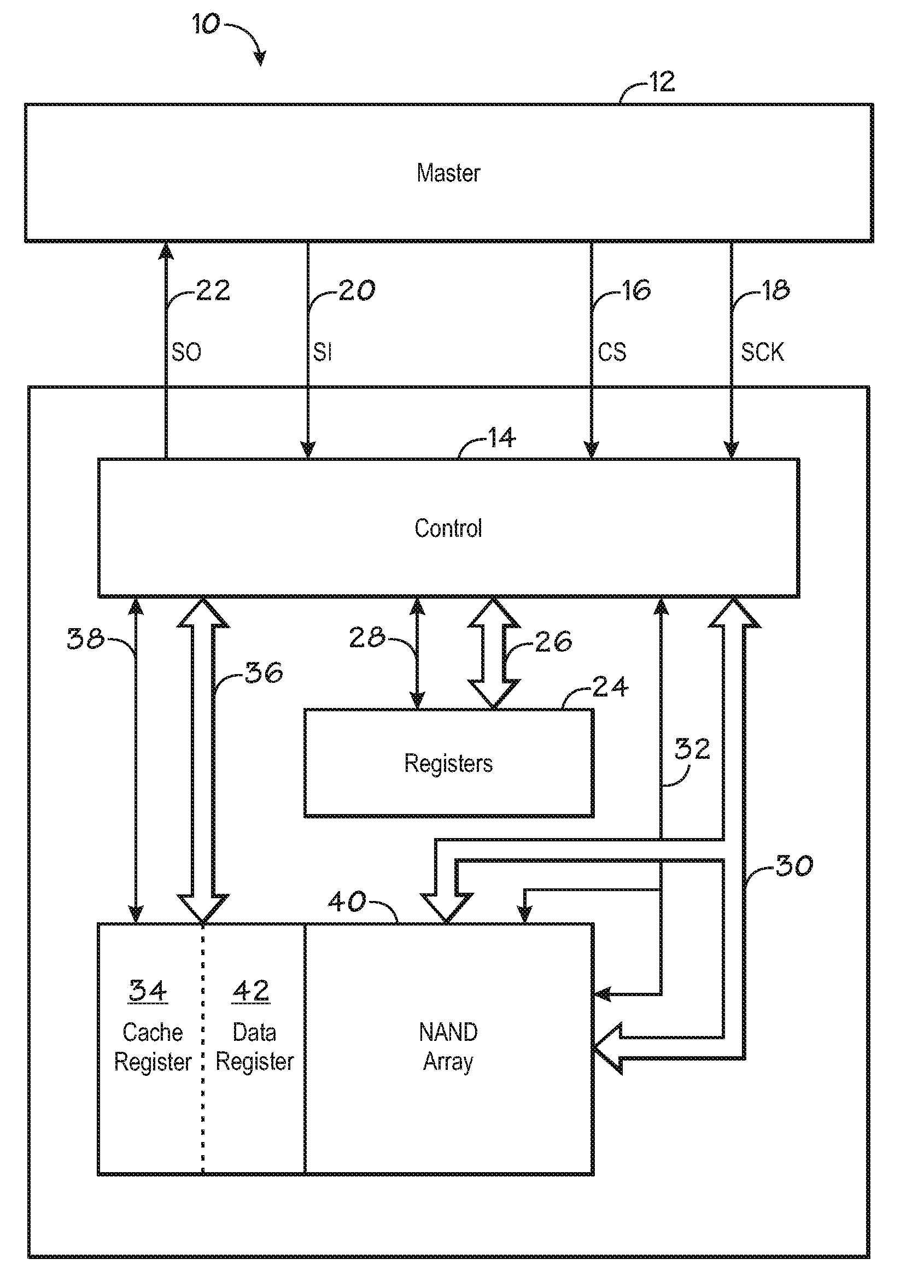
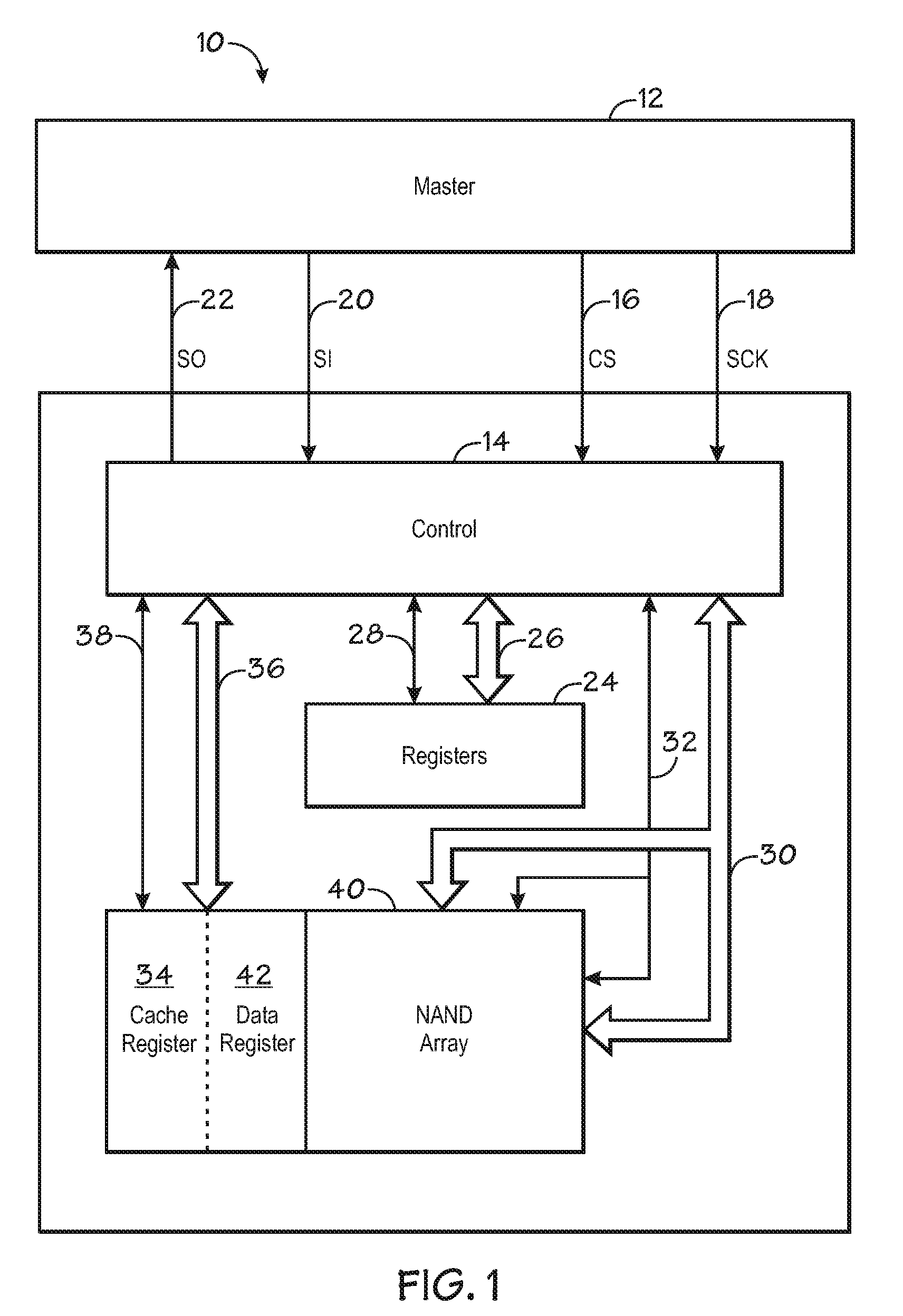
[0022]Referring to FIG. 1, an SPI NAND memory device 10 interfaces with a master 12 using a serial peripheral interface (SPI) protocol. Controller 14 includes four interface pins including a chip select (CS) pin to receive a chip select signal CS 16, a clock (SCK) pin to receive a clock signal SCK 18, a slave in (SI) data input pin to receive an input signal SI 20, and a slave out (SO) data output pin to output an output signal SO 22. Data transfer between master 12 and controller 14 takes place serially across input signal SI 20 and output signal SO 22.

[0023]The master 12 may enable the controller 14 by setting chip select signal CS 16 from high to low. After enabling the controller 14, master 12 may send a clock signal SCK 18 and a corresponding data signal SI 20. Each bit transmitted by SI 20 (and SO 22) may be synchronous to either a rising or falling edge of clock signal SCK 18. For illustrative purposes, memory device 10 inputs data on SI 20 latched on a rising clock edge and ...


PUM


Abstract

The invention includes a system and method of modifying a setting of a NAND flash memory device using serial peripheral interface (SPI) communication from a master to the NAND flash memory device. One embodiment generally includes sending an enable signal to a first memory circuit input, sending a clock signal to a second memory circuit input, sending a command signal synchronized to the clock signal to a third memory circuit input, sending a memory register address signal synchronized to the clock signal to the third memory circuit input, and sending a setting signal synchronized to the clock signal to the third memory circuit input.

Description

BACKGROUND[0001]1. Field of the Invention[0002]Embodiments of the present invention relate generally to accessing and modifying settings of a NAND flash memory device, and particularly to accessing and modifying settings of a NAND flash memory device configured for interconnection via serial peripheral interface.[0003]2. Description of the Related Art[0004]Generally, most NAND flash memory devices employ parallel communication between a NAND flash device and a host device across a multitude of input pins. Though effective, the quantity of pins vastly increases the amount of space a NAND flash memory device occupies on an integrated circuit (IC) chip. As an alternative to parallel communication, serial communication may reduce the number of interconnections. However, critical functionality may be reduced as the quantity of input pins decreases.[0005]Serial peripheral interface (SPI) permits a synchronous serial data link between a master and one or more slave devices. For a synchrono...

Claims


Application Information

Patent Timeline
Patent Type & Authority Applications(United States)
IPC IPC(8): G11C8/18G11C16/06
CPCG06F13/1694G06F3/0679G06F3/0629G06F3/0619G11C16/06G06F12/145G06F2212/1052G11C7/1021G11C7/1072
Inventor PEKNY, THEODORE T.TSAI, VICTOR Y.
Owner MICRON TECH INC
Why Eureka
Try Eureka