

Polishing Composition for CMP and device wafer producing method using the same
a technology of polishing composition and composition, which is applied in the direction of manufacturing tools, lapping machines, other chemical processes, etc., can solve the problems of reducing the current-carrying capacity and the use of conventional nonionic surfactants such as polyoxyalkylene, and achieve the effect of reducing, minimizing, or eliminating scratches
- Summary
- Abstract
- Description
- Claims
- Application Information
AI Technical Summary
Benefits of technology
Problems solved by technology
Method used
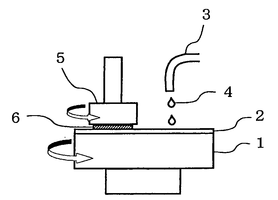
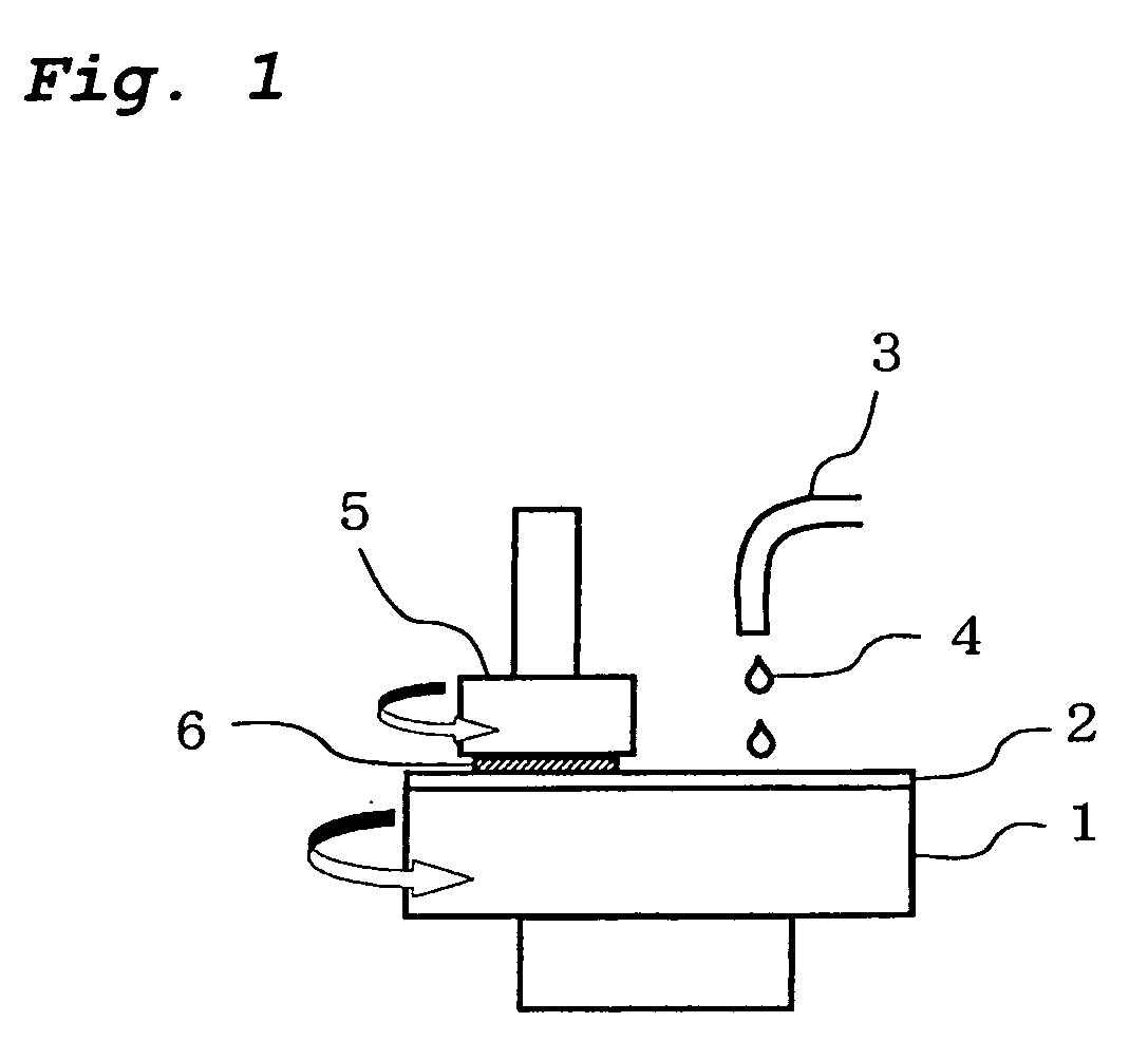
Image

Examples
example 1
[0084]Polishing composition for CMP 1 was prepared by mixing 4.0 parts by weight of Polyglycerol Derivative (A1), 20 parts by weight of the abrasive slurry prepared in Preparation Example (preparation of abrasive slurry), 0.2 part by weight of aqueous ammonia as a pH adjuster, and 200 ml of ion-exchanged water using a mixer (“T.K. HOMO MIXER”, PRIMIX Corporation, Japan).
example 2
[0085]Polishing composition for CMP 2 was prepared by mixing 4.0 parts by weight of Polyglycerol Derivative (A2), 20 parts by weight of the abrasive slurry prepared in Preparation Example (preparation of abrasive slurry), 0.2 part by weight of aqueous ammonia as a pH adjuster, and 200 ml of ion-exchanged water using a mixer (“T.K. HOMO MIXER”, PRIMIX Corporation, Japan).
example 3
[0086]Polishing composition for CMP 3 was prepared by mixing 4.0 parts by weight of Polyglycerol Derivative (A3), 20 parts by weight of the abrasive slurry prepared in Preparation Example (preparation of abrasive slurry), and 200 ml of ion-exchanged water using a mixer (“T.K. HOMO MIXER”, PRIMIX Corporation, Japan).
PUM
| Property | Measurement | Unit |
|---|---|---|
| degree of polymerization | aaaaa | aaaaa |
| total weight | aaaaa | aaaaa |
| abrasive | aaaaa | aaaaa |
Abstract
Description
Claims
Application Information