Structure and method for fabricating self-aligned metal contacts

a technology of metal contacts and metal contacts, which is applied in the direction of basic electric elements, electrical equipment, and semiconductor devices, etc., can solve the problems of reducing the performance of transistors, difficult to etch contact vias and avoid gate-to-via, and high undesirable effects

Inactive Publication Date: 2009-04-30
AURIGA INNOVATIONS INC
View PDF35 Cites 35 Cited by
  • Summary
  • Abstract
  • Description
  • Claims
  • Application Information

AI Technical Summary

Benefits of technology

[0010]at least one field effect transistor located on a surface of a semiconductor substrate, said at least one field effect transistor including a gate conductor stack comprising a lower layer of polysilicon and an upper layer of a first metal semiconduct

Problems solved by technology

It is, however, difficult to etch contact vias and to avoid gate-to-via shorts when the size of the via opening is small and spacing between gates and vias is small.
This degrades the performance of the transistor and, as such, is highly undesirable.
The gate-to-via shorts reduce chip yields and then

Method used


Image

  • Structure and method for fabricating self-aligned metal contacts
  • Structure and method for fabricating self-aligned metal contacts
  • Structure and method for fabricating self-aligned metal contacts

Examples


Embodiment Construction

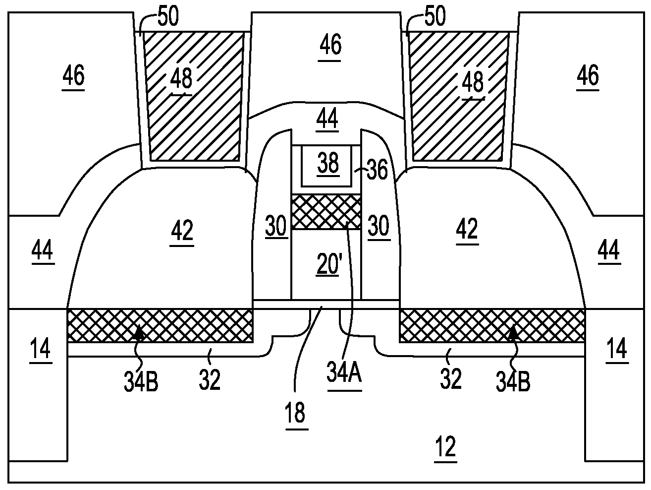
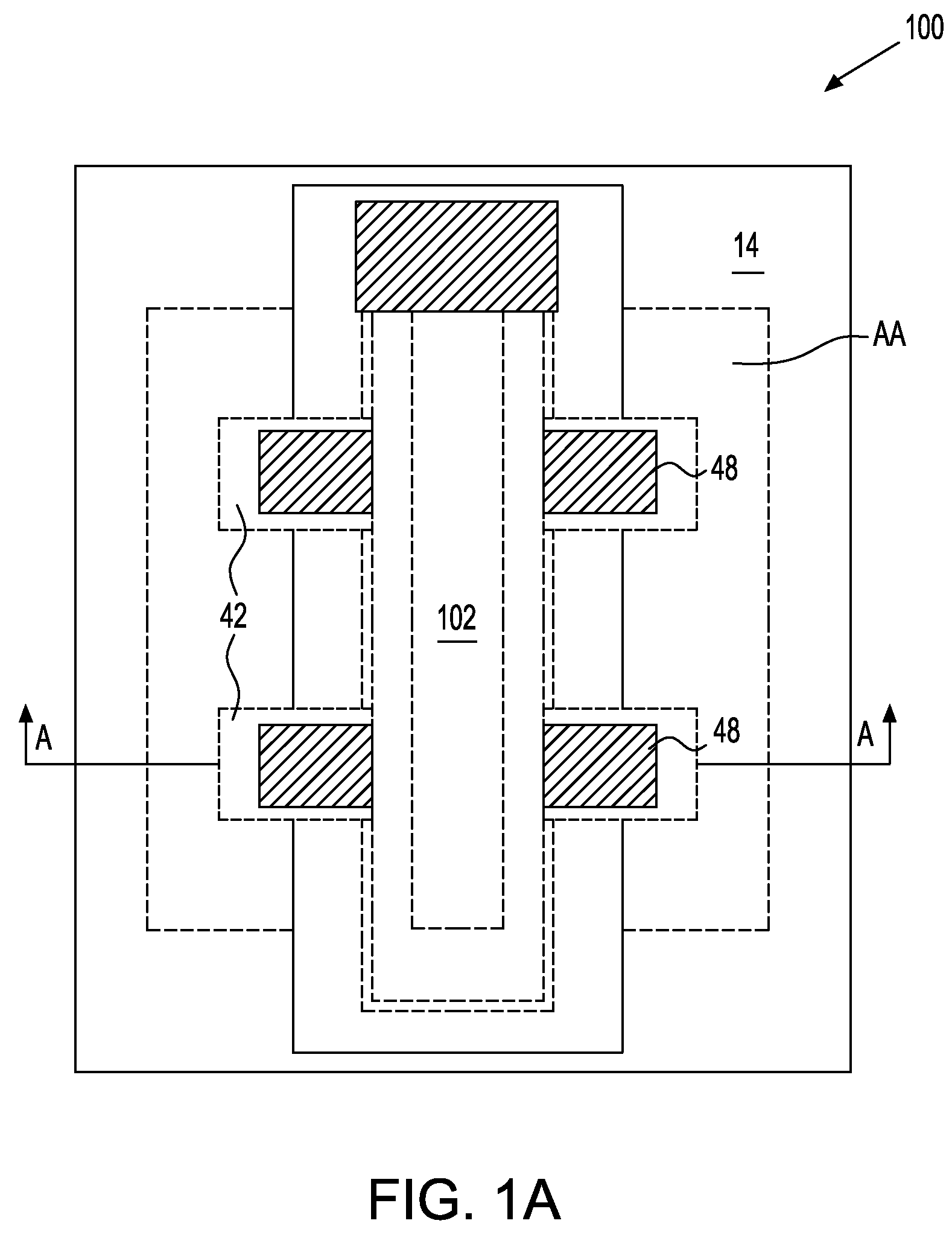
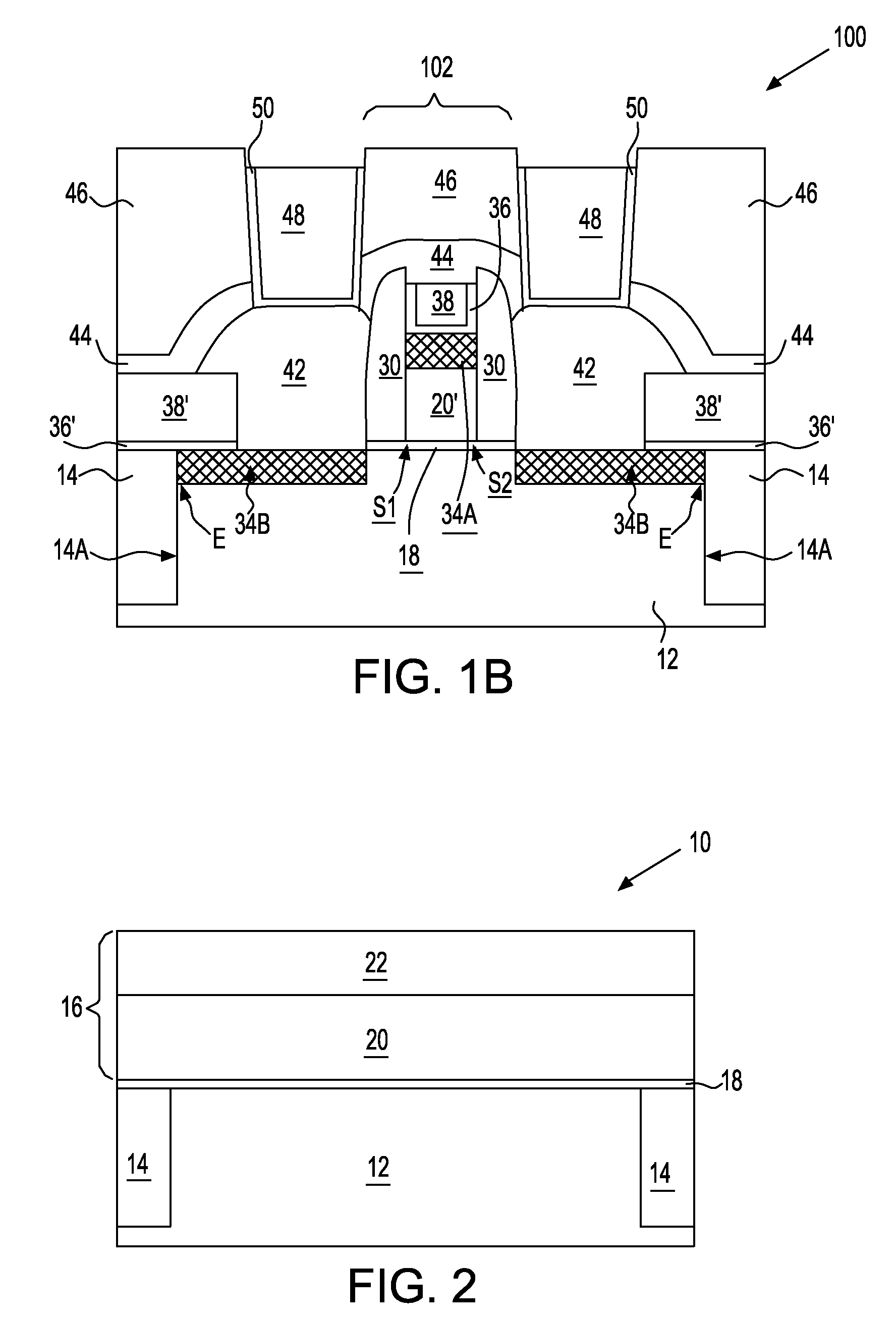
[0040]The present invention, which provides a semiconductor structure having improved device performance and chip yield as a result of a stressed layer located atop a gate conductor stack and a metallic contact located atop metal semiconductor alloy-containing source / drain diffusion regions and a method of fabricating the same, will now be described in greater detail by referring to the following discussion and drawings that accompany the present application. It is noted that the drawings of the present application are provided for illustrative purposes only and, as such, the drawings are not drawn to scale.

[0041]In the following description, numerous specific details are set forth, such as particular structures, components, materials, dimensions, processing steps and techniques, in order to provide a thorough understanding of the present invention. However, it will be appreciated by one of ordinary skill in the art that the invention may be practiced without these specific details....


PUM


Abstract

A semiconductor structure including at least one transistor is provided which has a stressed channel region that is a result of having a stressed layer present atop a gate conductor that includes a stack comprising a bottom polysilicon (polySi) layer and a top metal semiconductor alloy (i.e., metal silicide) layer. The stressed layer is self-aligned to the gate conductor. The inventive structure also has a reduced external parasitic S/D resistance as a result of having a metallic contact located atop source/drain regions that include a surface region comprised of a metal semiconductor alloy. The metallic contact is self-aligned to the gate conductor.

Description

FIELD OF THE INVENTION[0001]The present invention relates to a semiconductor structure. More particularly, the present invention relates to a semiconductor structure having self-aligned metal via contacts.BACKGROUND OF THE INVENTION[0002]Field effect transistors (FETs) are the basic building block of today's integrated circuit. Such transistors can be formed in conventional bulk substrates (such as silicon) or in semiconductor-on-insulator (SOI) substrates.[0003]State of the art metal oxide semiconductor (MOS) transistors are fabricated by depositing a gate stack material over a gate dielectric and a substrate. Generally, the MOS transistor fabrication process implements lithography and etching processes to define the conductive, e.g., poly-Si, gate structures. The gate structure and substrate are thermally oxidized, and, after this, source / drain extensions are formed by implantation. Sometimes the implant is performed using a spacer to create a specific distance between the gate an...

Claims


Application Information

Patent Timeline
IPC IPC(8): H01L21/336H01L29/78
CPCH01L21/28061H01L29/66545H01L29/7845H01L29/7843H01L29/7833
Inventor ZHU, HUILONGRAUSCH, WERNER
Owner AURIGA INNOVATIONS INC
Why Eureka
Try Eureka