Wafer-level underfill process using over-bump-applied resin

a technology of underfill and wafer, which is applied in the direction of electrical equipment, semiconductor devices, semiconductor/solid-state device details, etc., can solve the problems of difficult cleaning step and limited reliability of the package containing the underfill, and achieve excellent underfill adhesion, improve the wluf process, and facilitate the thickness of the wluf material

Inactive Publication Date: 2009-04-30
IBM CORP
View PDF7 Cites 9 Cited by
  • Summary
  • Abstract
  • Description
  • Claims
  • Application Information

AI Technical Summary

Benefits of technology

[0012]Pursuant to the invention, a novel WLUF process resides in employing wafers that have solder bumps of essentially equal height, such as are obtained using the C4NP process (Controlled Collapse Chip Connection—new process), as is known in the prior art. This process allows for the provision of wafers in which the bump height is very uniform, considerably more so than in plated bumps. The presence of uniform bump height is advantageous in the WLUF process since it ensures that all bumps are coated to a uniform height. This facilitates that the thickness of the WLUF material through which the bumps require to be pushed through in order to make contact with the pads of the substrate, can be selected so as to be uniform. It further ensures that substantially all bumps will make contact with the corresponding substrate pads after the bumps have pushed through the coating. Moreover, the coating of the bumps with the WLUF material protects the bumps from excessive oxidation thereof.
[0013]Another advantage obtained by the present invention is to improve the WLUF process by employing wafers which were first tested prior to the wafer-level underfill (WLUF) material being applied to the bumped wafer in a manner that covers the majority of the bumps. This is accomplished by using methods known in the field to identify known-good dies.
[0014]The present invention further enables the achievement of an excellent degree of underfill adhesion by cleaning of the wafer before WLUF application. For example, a chip is normally cleaned after joining it to the substrate through using a flux to allow for C4 reflow. This cleaning step is difficult, particularly for small C4 bump sizes and large chips, since it is difficult to get the cleaning solutions into and out of small gaps. However, cleaning is absolutely necessary to be able to ensure good underfill adhesion, since without the presence of good adhesion, the reliability of the package containing the underfill is severely limited. Cleaning steps that are taken may involve cleaning with diluted acids, such as sulphuric acid, washing with an aqueous detergent solution followed by a DI rinse and rinsing with IPA, and / or oxygen plasma etching. In the WLUF process pursuant to the current invention, a bumped wafer is prepared for WLUF deposition by cleaning the wafer after bumping through processes that are typical for after bump and / or after solder join operations; whereby the wafers are then baked in order to remove volatiles from the surface and / or the passivation layer (particularly if there is used a polymeric passivation layer, such as photosensitive polyimide) just before application of the WLUF material, so that the bumps are largely coated by a layer of WLUF material.
[0015]Moreover, the present invention produces wafers that are protected by the WLUF material during wafer thinning and during subsequent handling. Since wafers are often thinned down to between 300 and 30 microns they tend to become quite fragile. Adding an organic, b-staged resin with a modulus of about 0.5-1 GPa and a thickness that exceeds the height of the bumps by 1-100 μm, imparts a significant degree of robustness to the wafer, and thereby decreases possible damage due to handling. The B-staged WLUF coating also protects the extremely fragile chip interconnect structure; an aspect that may be particularly advantageous in the development of future, low-k interlayer dielectric interconnects, whereas the WLUF also protects the solder bumps from excessive oxidation during storage.
[0016]Finally, chips, which are protected by a WLUF material, enjoy the benefit of the underfill already during the first cool down after chip join. Fragile low-k dielectric interconnect structures are easily broken during this first cool down through the stresses imparted by the CTE mismatch of the chip and substrate, however, since the WLUF material substantially or fully cures during chip join it provides the function of the underfilling extending reliability and life expectancy ab initio.

Problems solved by technology

This cleaning step is difficult, particularly for small C4 bump sizes and large chips, since it is difficult to get the cleaning solutions into and out of small gaps.
However, cleaning is absolutely necessary to be able to ensure good underfill adhesion, since without the presence of good adhesion, the reliability of the package containing the underfill is severely limited.

Method used


Image

  • Wafer-level underfill process using over-bump-applied resin
  • Wafer-level underfill process using over-bump-applied resin
  • Wafer-level underfill process using over-bump-applied resin

Examples


Embodiment Construction

[0035]Throughout the several drawing views, elements and structures which are similar or identical to each other, will be designated with the same reference numerals.

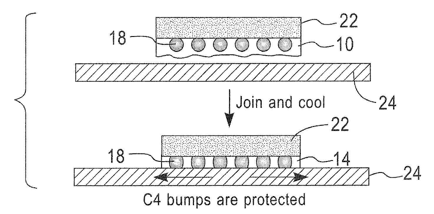
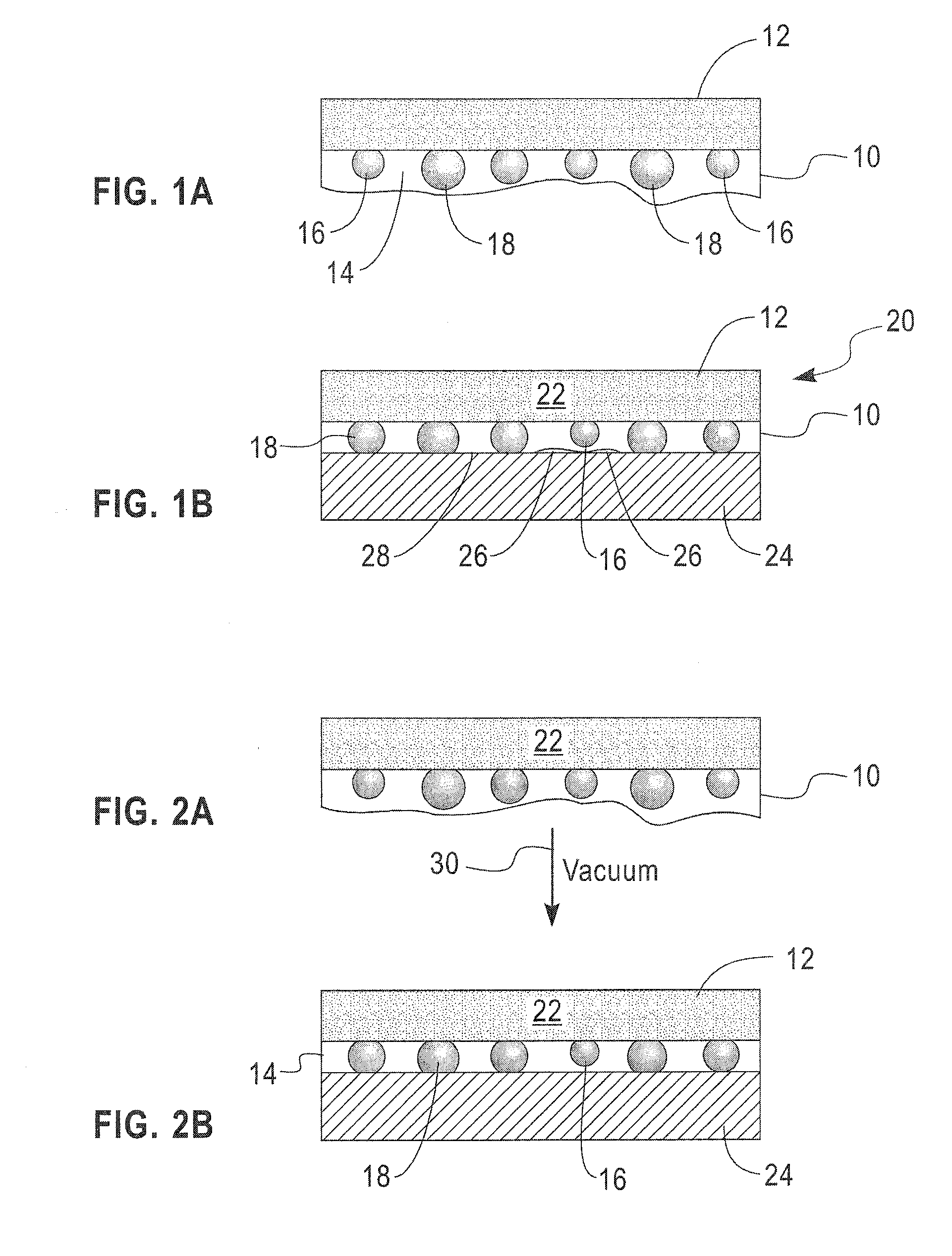
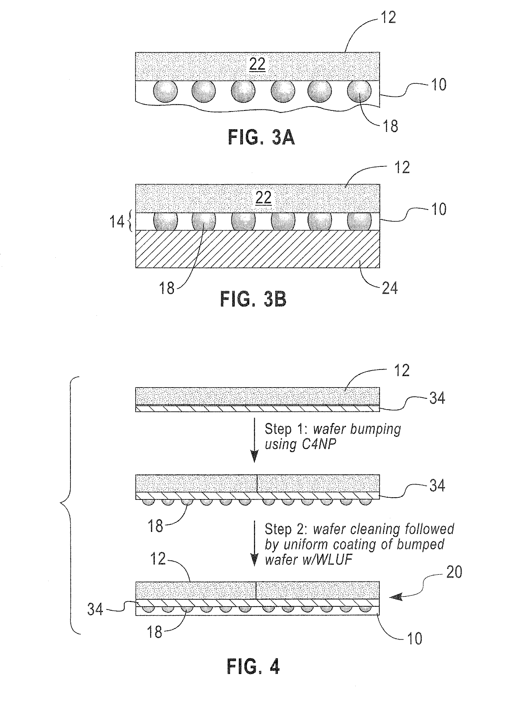
[0036]Referring in specific detail to the drawings, the inventive over-bump wafer-level underfill process requires that the WLUF (wafer-level underfill) material 10 is applied to a fully bumped wafer 12 so that a layer 14 of the WLUF material covers the solder bumps 16, 18. If the WLUF layer 14 is uniform and flat, irrespective if the solder bumps 16, 18 are different in size, and does not show large peaks and valleys, little or no air is entrapped during the subsequent joining of singulated WLUF coated chips to substrates. Air entrapment is undesirable since it reduces the reliability of the finished semiconductor package 20.

[0037]Plated bumps 16, 18 tend to exhibit significant bump height variations, as shown in FIG. 1a. When a WLUF material coats wafers 12 with such plated bumps 16, 18 and chips 22 obtained from such...


PUM


Abstract

A process of fabricating wafer-level underfilled microelectronic packages using over-bump application of a self-fluxing resin to a wafer, b-staging of the resin, dicing of the coated wafer, and joining the diced chips to substrates producing wafer-level underfilled microelectronic flip-chip packages. Moreover, provided are microelectronic packages, which are produced in accordance with the inventive process.

Description

BACKGROUND OF THE INVENTION[0001]1. Field of the Invention[0002]The present invention relates to a process of fabricating wafer-level underfilled microelectronic packages using over-bump application of a self-fluxing resin to a wafer, b-staging of the resin, dicing of the coated wafer, and joining the diced chips to substrates producing wafer-level underfilled microelectronic flip-chip packages. Moreover, the invention is further directed to the provision of microelectronic packages, which are produced in accordance with the inventive process.[0003]Flip Chip technology is the fastest growing chip interconnect technology today because it allows for very large numbers of I / Os. Thus the footprint of chips with low numbers of I / O's can be made very small. This also holds true for associated electronic packages, such as chip-scale packages.[0004]A major advantage of flip chip technology resides in that it can utilize the total chip area in order to provide the I / O connections, while cont...

Claims


Application Information

Patent Timeline
Patent Type & Authority Applications(United States)
IPC IPC(8): H01L21/58H01L23/12
CPCH01L21/563H01L24/81H01L2924/10253H01L2224/1181H01L24/29H01L2924/0665H01L2924/014H01L2924/01076H01L24/83H01L24/90H01L2224/0401H01L2224/0603H01L2224/1403H01L2224/16H01L2224/274H01L2224/73203H01L2224/81801H01L2224/83102H01L2224/83191H01L2224/83194H01L2224/83856H01L2224/92125H01L2924/01005H01L2924/01013H01L2224/2919H01L2924/01006H01L2924/01019H01L2924/00H01L2224/14H01L2224/73104
Inventor FEGER, CLAUDIUSLABIANCA, NANCY C.
Owner IBM CORP
Why Eureka
Try Eureka