Touch Screen

a touch screen and touch technology, applied in the field of touch screens, can solve the problems of high cost, affecting the use of the system, and affecting the user's experience, so as to improve the drawback of transformation damage, prolong the use time of the product, and fast transmission of signals

Inactive Publication Date: 2009-04-30
LUNGHWA UNIVERSITY OF SCIENCE AND TECHNOLOGY
View PDF4 Cites 13 Cited by
  • Summary
  • Abstract
  • Description
  • Claims
  • Application Information

AI Technical Summary

Benefits of technology

[0008]The present invention receives the signals from the wave sensor that employs the concept of the reflection of the light, sound, or supersonic, and the signals are calculated by the core logic circuit to obtain the position coordinate of an object. And then a display module is employed to show the moving path of the object in the manner of an image or line on a screen. Beside the advantage of the fast transmission of signals, it can improve the drawback of the transformation damage caused by undergoing the repeated stress for the conventional touch screen so as to extend the usage time of the product, and effectively reduce the manufacturing cost to reach the goal of popularization.

Problems solved by technology

However, no matter it is the resistor-type or capacitor-type touch screen, the polyester or conducting layer is aging under the condition of pressing for a long time to cause the sensitivity reduction.
If the multi-point touching, two or more touch points touching, is performed, the points may not be distinguished, or the error caused by the deviation of the positioning analysis is so big to bother the user a lot.
There is a drawback of high cost as well for the system.

Method used


Image

  • Touch Screen
  • Touch Screen
  • Touch Screen

Examples


Embodiment Construction

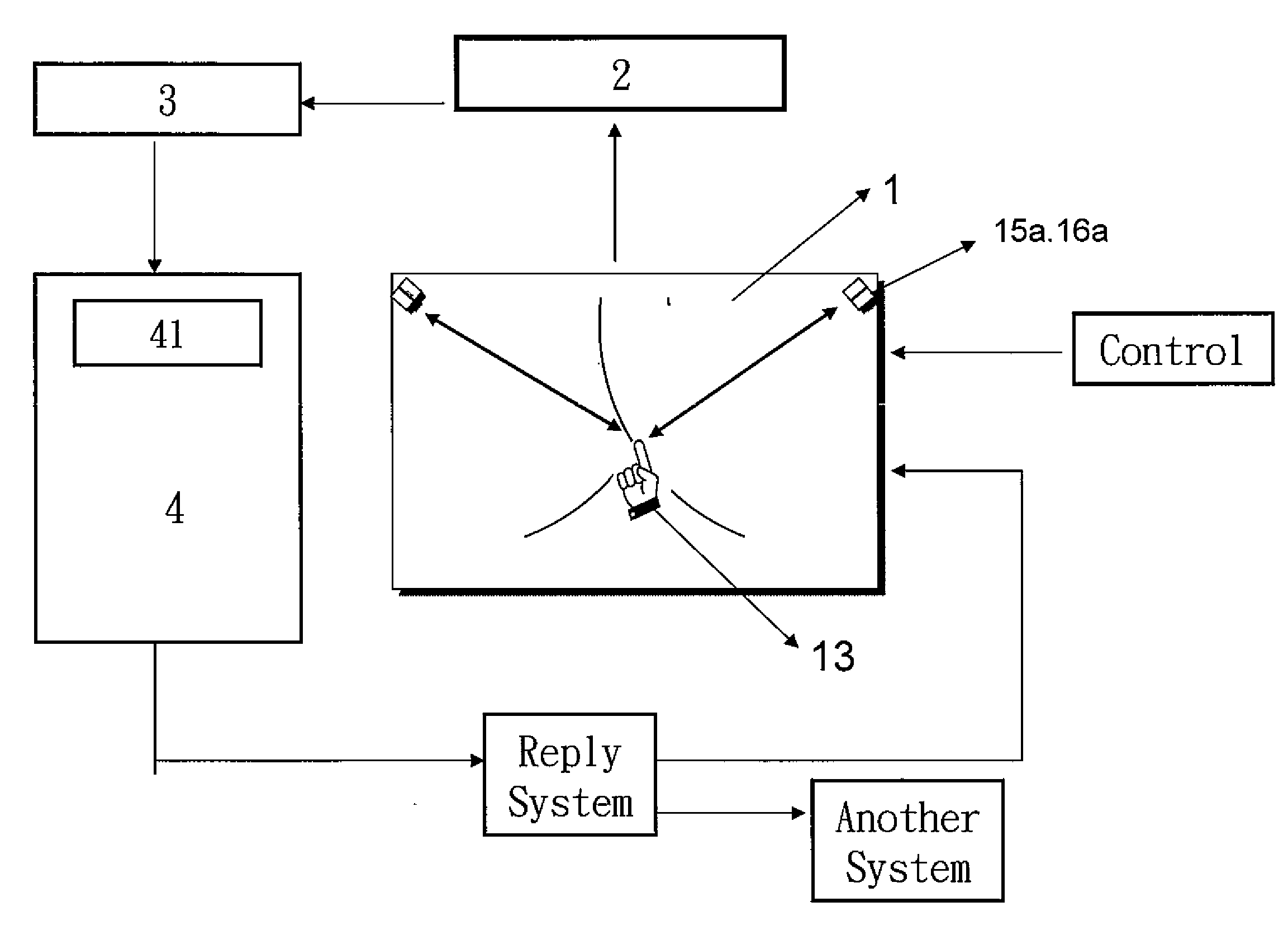
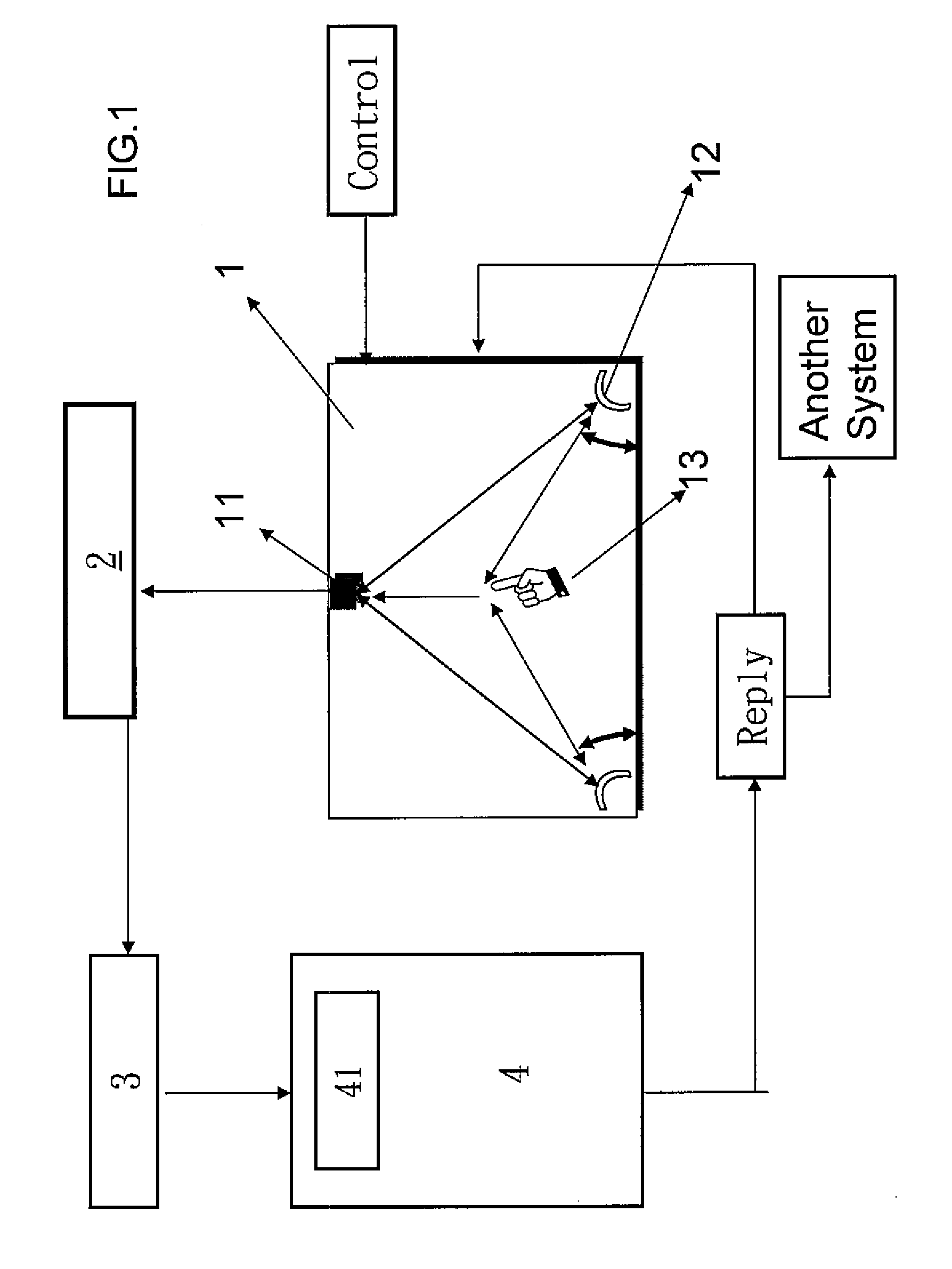
[0016]Please referring to FIG. 1, there is a screen 1 and a CMOS optical image sensor 11 locates at the proper position on the screen 1. There are two convex mirrors 12 at the proper positions corresponding to the CMOS optical image sensor 11. The arrangement of the devices mentioned above forms an image sensing net. When an object 13 enters the image sensing net, the CMOS optical image sensor 11 retrieves the object images through or not through the convex mirrors 13 respectively. The object images are transmitted to the CMOS image retrieving circuit 2 which is electrically connected to the CMOS optical image sensor 11. And then the object images are transmitted to the image analysis circuit 4 through the noise filter 3. The two object images are compared by the core logic circuit to calculate for positioning the object 13 corresponding to the screen 1.

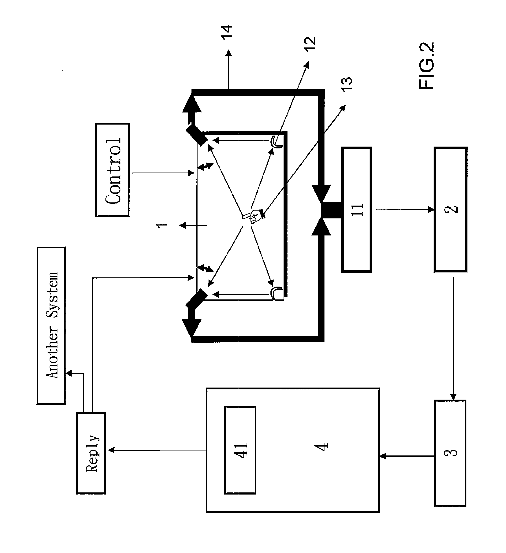
[0017]Referring to FIG. 2, it is another embodiment of the system shown in FIG. 1. The CMOS optical image sensor 11 is excluded fro...


PUM


Abstract

The present invention provides the system design of the positioning analysis of a touch screen. It receives the signals from the wave sensor that employs the concept of the reflection of the light, sound, or supersonic, and the signals are calculated by the core logic circuit to obtain the position coordinate of an object. And then a display module is employed to show the moving path of the object in the manner of an image or line on a screen. The wave sensor may be implemented by a CMOS optical image sensor, infrared sensor, or supersonic sensor. The CMOS (Complementary metal oxide semiconductor) optical image sensor may additionally comprise fibers to transmit the optical wave to the CMOS sensor smoothly.

Description

BACKGROUND OF THE PRESENT INVENTION [0001]1. Field of Invention[0002]The present invention relates to a touch screen, particularly to the touch screen employing the concept of the detection of the wave reflection.[0003]2. Description of Related Arts[0004]The conventional touch screen may be classified to the resister-type and capacitor-type. The resister-type touch screen includes a polyester layer on the surface with a conducting metal film inside. The bottom of the touch screen is a glass panel covered by the conducting material stuck on the CRT (cathode-ray tube) or LCD (liquid crystal display). There are tiny “separating points” formed by polyester to separate the glass panel and the polyester layer. There is a controller alone the X axis and Y axis of the glass panel separately which can apply small voltage gradients. Whenever a finger touches the screen, the two conducting layers are pressed to touch each other. Therefore, the electronic apparatus can detect the X-Y coordinate...

Claims


Application Information

Patent Timeline
Patent Type & Authority Applications(United States)
IPC IPC(8): G06F3/042
CPCG06F3/0428
Inventor WENG, WEN-PINTZU, CHUNG-HSING
Owner LUNGHWA UNIVERSITY OF SCIENCE AND TECHNOLOGY
Why Eureka
Try Eureka