

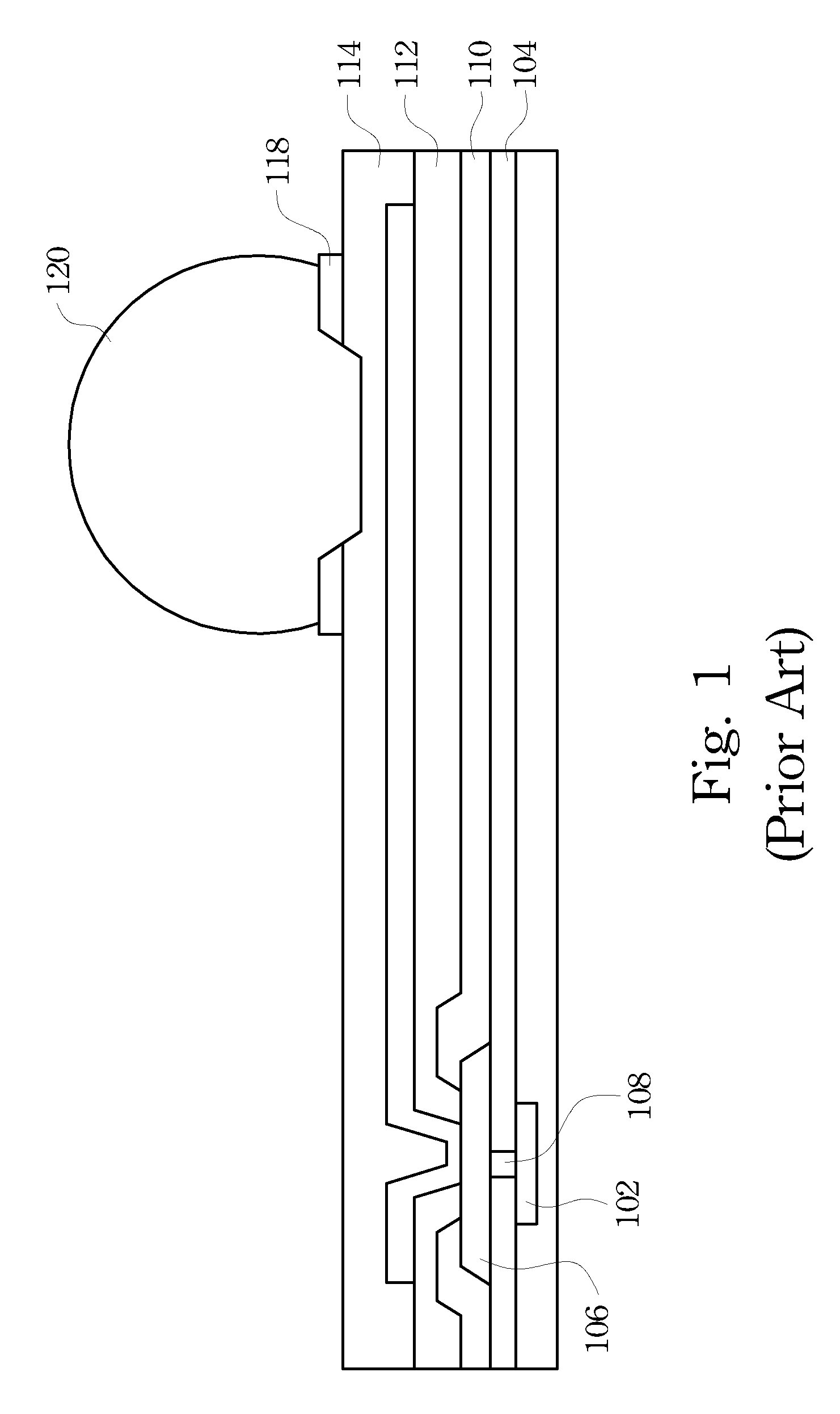
Back End Integrated WLCSP Structure without Aluminum Pads
a technology of back end and aluminum pad, applied in the field of back end of processes, can solve problems such as increasing rc delay, and achieve the effect of reducing rc delay and reducing manufacturing cos
- Summary
- Abstract
- Description
- Claims
- Application Information
AI Technical Summary
Benefits of technology
Problems solved by technology
Method used
Image

Examples
Embodiment Construction
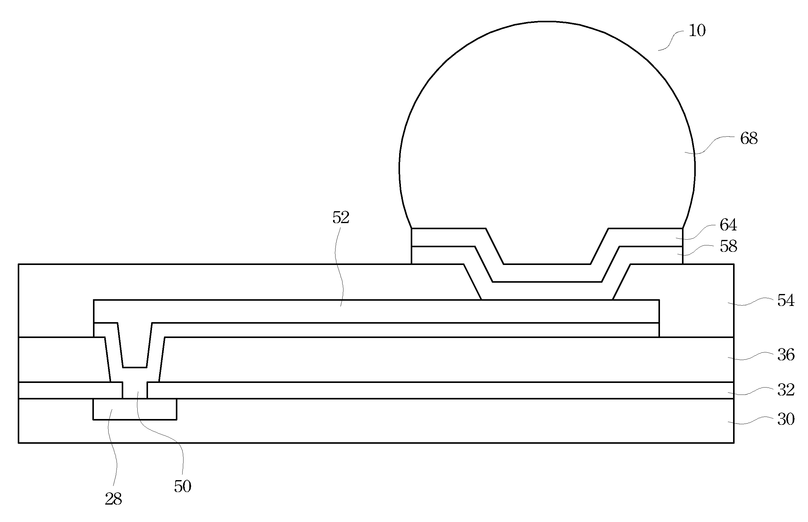
[0016]The making and using of the presently preferred embodiments are discussed in detail below. It should be appreciated, however, that the present invention provides many applicable inventive concepts that can be embodied in a wide variety of specific contexts. The specific embodiments discussed are merely illustrative of specific ways to make and use the invention, and do not limit the scope of the invention.
[0017]A novel integrated circuit structure formed in a back end of the process and the method of forming the same are provided. The intermediate stages of manufacturing a preferred embodiment of the present invention are illustrated. The variations of the preferred embodiments are then discussed. Throughout the various views and illustrative embodiments of the present invention, like reference numbers are used to designate like elements.
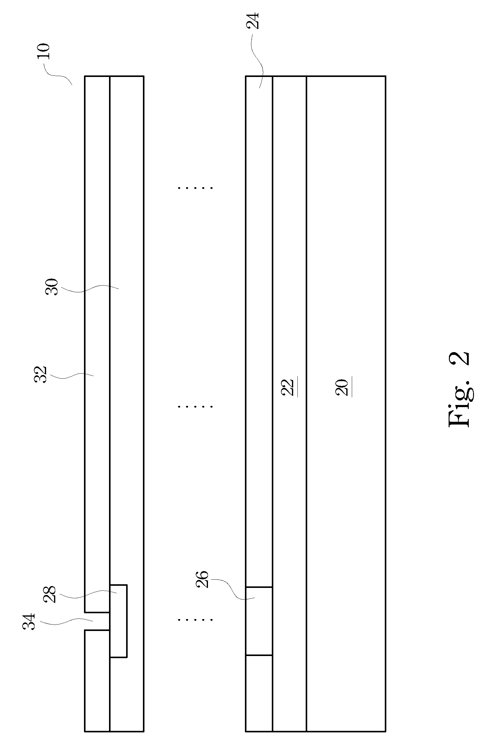
[0018]Referring to FIG. 2, wafer 10, which includes semiconductor substrate 20, is provided. Semiconductor substrate 20 may be a bulk silicon...
PUM
 Abstract
Description
Claims
Application Information